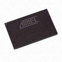
AT91FR40161-CI Atmel, AT91FR40161-CI Datasheet - Page 10

AT91FR40161-CI
Manufacturer Part Number
AT91FR40161-CI
Description
IC MCU ARM7 2M FLASH 120-BGA
Manufacturer
Atmel
Series
AT91SAMr
Datasheet
1.AT91FR40161-CI.pdf
(22 pages)
Specifications of AT91FR40161-CI
Core Processor
ARM7
Core Size
16/32-Bit
Speed
33MHz
Connectivity
EBI/EMI, UART/USART
Peripherals
WDT
Number Of I /o
32
Program Memory Size
2MB (1M x 16)
Program Memory Type
FLASH
Ram Size
136K x 8
Voltage - Supply (vcc/vdd)
2.7 V ~ 3.6 V
Oscillator Type
External
Operating Temperature
-40°C ~ 85°C
Package / Case
120-BGA
Lead Free Status / RoHS Status
Contains lead / RoHS non-compliant
Eeprom Size
-
Data Converters
-
Available stocks
Company
Part Number
Manufacturer
Quantity
Price
Company:
Part Number:
AT91FR40161-CI
Manufacturer:
TI
Quantity:
101
Memory Controller
Internal Memories
Boot Mode Select
10
AT94FR40161
ARM7TDMI core responds with a non-JTAG chip ID that identifies the microcontroller.
This is not fully IEEE1149.1 compliant.
The ARM7TDMI processor address space is 4 Gbytes. The memory controller decodes
the internal 32-bit address bus and defines three address spaces:
•
•
•
In any of these address spaces, the ARM7TDMI operates in little-endian mode only.
The AT91FR40161 microcontroller integrates 8 Kbytes of primary internal SRAM that is
32 bits wide and single clock cycle accessible. This memory bank is mapped at address
0x0 (after the remap command), allowing ARM7TDMI exception vectors between 0x0
and 0x20 to be modified by the software. The rest of the bank can be used for stack allo-
cation (to speed up context saving and restoring), or as data and program storage for
critical algorithms. Byte (8-bit), half-word (16-bit) or word (32-bit) accesses are sup-
ported and are executed within one cycle. Fetching Thumb or ARM instructions is
supported and internal memory can store twice as many Thumb instructions as ARM
ones.
The AT91FR40161 also integrates an extended memory bank of 128 Kbytes at address
0x0010 0000. Placing the SRAM on-chip and using the 32-bit data bus bandwidth maxi-
mizes the microcontroller performance and minimizes the system power consumption.
The 32-bit bus increases the effectiveness of the use of the ARM instruction set, and the
ability of processing data that is wider than 16-bit, thus making optimal use of the
ARM7TDMI advanced performance.
Being able to dynamically update application software in the 128 Kbyte SRAM adds an
extra dimension to the AT91FR40161. In order to prevent accidental write to the
extended SRAM while the application is running, a write detection feature has been
implemented.
The AT91FR40161 also integrates a 2 Mbyte Flash memory that is accessed via the
External Bus Interface. All data, address and control lines, except for the Chip Select
signal, are connected within the device.
The ARM reset vector is at address 0x0. After the NRST line is released, the
ARM7TDMI executes the instruction stored at this address. This means that this
address must be mapped in nonvolatile memory after the reset. The input level on the
BMS pin during the last 10 clock cycles before the rising edge of the NRST selects the
type of boot memory (see Table 3).
If the embedded Flash memory is to be used as boot memory, the BMS input must be
pulled down externally and NCS0 must be connected to NCSF externally.
The pin BMS is multiplexed with the I/O line P24 that can be programmed after reset like
any standard PIO line.
Table 3. Boot Mode Select
Internal memories in the four lowest megabytes
Middle space reserved for the external devices (memory or peripherals) controlled
by the EBI
Internal peripherals in the four highest megabytes
BMS
1
0
Boot Memory
Internal 32-bit extended SRAM
External 16-bit memory on NCS0
6040B–ATARM–03/04


