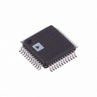
ADUC7032BSTZ-8V-RL Analog Devices Inc, ADUC7032BSTZ-8V-RL Datasheet - Page 29

ADUC7032BSTZ-8V-RL
Manufacturer Part Number
ADUC7032BSTZ-8V-RL
Description
IC BATTERY SENSOR PREC 48-LQFP
Manufacturer
Analog Devices Inc
Series
MicroConverter® ADuC7xxxr
Datasheet
1.ADUC7032BSTZ-8V-RL.pdf
(128 pages)
Specifications of ADUC7032BSTZ-8V-RL
Core Processor
ARM7
Core Size
16/32-Bit
Speed
20.48MHz
Connectivity
LIN, SPI, UART/USART
Peripherals
POR, PSM, Temp Sensor, WDT
Number Of I /o
9
Program Memory Size
96KB (96K x 8)
Program Memory Type
FLASH
Ram Size
6K x 8
Voltage - Supply (vcc/vdd)
3.5 V ~ 18 V
Data Converters
A/D 2x16b
Oscillator Type
Internal
Operating Temperature
-40°C ~ 105°C
Package / Case
48-LQFP
Lead Free Status / RoHS Status
Lead free / RoHS Compliant
Eeprom Size
-
Other names
ADUC7032BSTZ-8V-RLCT
Available stocks
Company
Part Number
Manufacturer
Quantity
Price
Company:
Part Number:
ADUC7032BSTZ-8V-RL
Manufacturer:
Analog Devices Inc
Quantity:
10 000
Preliminary Technical Data
Remap
The ARM exception vectors are all situated at the bottom of the
memory
0x00000020.
By default, after a reset, the Flash/EE memory is logically
mapped to address 0x00000000.
It is possible to logically REMAP the SRAM to address
0x00000000. This is done by a setting bit zero of the SYSMAP0
MMR, which is located at 0xFFFF0220. To revert Flash/EE to
0x00000000, bit zero of SYSMAP0 is cleared.
It may be desirable to remap RAM to 0x00000000 to optimize
the interrupt latency of the ADuC7032, as code may be run in
full 32bit ARM mode and at the maximum core speed. It should
be noted that when an exception occurs, the core will default to
ARM mode.
Remap operation
When a reset occurs on the ADuC7032, execution starts
automatically in the factory programmed internal configuration
SYSMAP0 Register :
Name :
Address :
Default Value :
Access :
Function :
memory
Bit
7-1
0
Description
Reserved
These bits are reserved and should be written as 0 by user code
Remap Bit.
Set by the user to remap the SRAM to 0x00000000.
Cleared automatically after reset to remap the Flash/EE memory to 0x00000000.
array,
from
SYSMAP0
0xFFFF0220
0x00
Read/Write Access
This 8-bit register allows user code to remap either RAM or Flash/EE memory space into the bottom of the ARM
address
space starting at location 0x00000000.
0x00000000
to
Table 8: SYSMAP0 MMR Bit Designations
address
Rev. PrD | Page 29 of 128
code. This so called kernel is hidden and cannot be accessed by
user code. If the ADuC7032 is in normal mode, it will execute
the power-on configuration routine of the kernel and then jump
to the reset vector address, 0x00000000, to execute the users
reset exception routine.
Because the Flash/EE is mirrored at the bottom of the memory
array at reset, the reset routine must always be written in
Flash/EE.
Precaution must be taken to execute the REMAP command
from the absolute Flash/EE address, and not from the mirrored,
remapped segment of memory, as this will be replaced by the
SRAM. If a remap operation is executed whilst operating code
from the mirrored location, Prefetch/Data aborts may occur or
the user may observe abnormal program operation.
This operation is reversible: the Flash/EE memory may be
remapped at address 0x00000000 by clearing bit zero of the
SYSMAP0 MMR. Precaution must again be taken to execute the
remap function from outside the mirrored area.
Any kind of reset will logically remap the Flash/EE memory to
the bottom of the memory array.
ADuC7032


