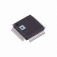
ADUC7032BSTZ-8V-RL Analog Devices Inc, ADUC7032BSTZ-8V-RL Datasheet - Page 97

ADUC7032BSTZ-8V-RL
Manufacturer Part Number
ADUC7032BSTZ-8V-RL
Description
IC BATTERY SENSOR PREC 48-LQFP
Manufacturer
Analog Devices Inc
Series
MicroConverter® ADuC7xxxr
Datasheet
1.ADUC7032BSTZ-8V-RL.pdf
(128 pages)
Specifications of ADUC7032BSTZ-8V-RL
Core Processor
ARM7
Core Size
16/32-Bit
Speed
20.48MHz
Connectivity
LIN, SPI, UART/USART
Peripherals
POR, PSM, Temp Sensor, WDT
Number Of I /o
9
Program Memory Size
96KB (96K x 8)
Program Memory Type
FLASH
Ram Size
6K x 8
Voltage - Supply (vcc/vdd)
3.5 V ~ 18 V
Data Converters
A/D 2x16b
Oscillator Type
Internal
Operating Temperature
-40°C ~ 105°C
Package / Case
48-LQFP
Lead Free Status / RoHS Status
Lead free / RoHS Compliant
Eeprom Size
-
Other names
ADUC7032BSTZ-8V-RLCT
Available stocks
Company
Part Number
Manufacturer
Quantity
Price
Company:
Part Number:
ADUC7032BSTZ-8V-RL
Manufacturer:
Analog Devices Inc
Quantity:
10 000
Preliminary Technical Data
HIGH VOLTAGE PERIPHERAL CONTROL
INTERFACE
The ADuC7032 integrates a number of high voltage circuit
functions which are controlled and monitored via a registered
interface consisting of 2 MMRs, namely, HVCON and HVDAT.
The HVCON register acts as a command byte interpreter
allowing the microcontroller to indirectly read or write 8-bit
data(the value in HVDAT) from/to one of 4 High voltage
status/configuration registers. It should be noted that these high
voltage registers are not MMRs but are so called ‘indirect’
registers that can only be accessed (as the name suggests)
indirectly via the HVCON and HVDAT MMRs.
The physical interface between the HVCON register and the
indirect high voltage registers is a 2 wire (data and clock) serial
interface based on a 2.56MHz serial clock. Therefore, there is a
finite, 10usecs(maximum) latency between the MCU core
writing a command into HVCON and that command or data
PERIPHERALS
ARM7
MCU
AND
IRQ3
(IRQEN[16])
HIGH-VOLTAGE
INTERFACE
WU DIAGNOSTIC I/P
LIN DIAGNOSTIC I/P
HVCON
STI DIAGNOSTIC I/P
HVDAT
MMRs
Figure 35 : High Voltage Interface, Top Level Block Diagram
HVCFG0[4]
HVCFG1[3]
HVCFG1[7]
HVCFG1[5]
SERIAL
SERIAL
CLOCK
P2.6
P2.5
DATA
Rev. PrD | Page 97 of 128
HIGH VOLTAGE
HIGH VOLTAGE
CONTROLLER
ATTENUATOR
CONTROLLER
CONTROLLER
DIAGNOSTIC
INTERFACE
INTERRUPT
BUFFER
SERIAL
AND
reaching the indirect high voltage registers. There is also a finite
10usecs latency between the MCU core writing a command into
HVCON and indirect register data being read back into the
HVDAT register. A busy bit (Bit0 of the HVCON when read by
MCU) can be polled by the MCU to confirm when a read/write
command has completed.
The following high voltage circuit functions are controlled and
monitored via this interface and Figure 35 below describes the
top-level architecture of the high voltage interface and related
circuits.
HVCFG1[6]
- Precision Oscillator
- Wake-Up pin functionality
- Power Supply Monitor
- Low Voltage Flag
- LIN Operating Modes
- High Voltage Diagnostics
- High Voltage Attenuator/Buffer Circuit
- High Voltage Temperature Monitor
PSM—HVSTA[5]
WU—HVSTA[4]
OVER TEMP—HVSTA[3]
LIN S-SCT—HVSTA[2]
STI S-SCT—HVSTA[1]
WU S-SCT—HVSTA[0]
WU DIAGNOSTIC O/P
HVMON[7]
STI DIAGNOSTIC O/P
HVMON[5]
LIN DIAGNOSTIC O/P
P2.4
HIGH-VOLTAGE
REGISTERS
(INDIRECT)
HVCFG0
HVCFG1
HVMON
HVSTA
MONITOR
HV TEMP
HVCFG0[6]
HVCFG0[3]
HVCFG0[2]
HVCFG0[1:0]
HVCFG0[5]
HVCFG0[4]
HVCFG1[4]
HVCFG1[4]
HVCFG1[3]
OSCILLATOR
PRECISION
CONTROL
CONTROL
MODES
WU I/O
STI I/O
ADuC7032
PSM
LVF
LIN


