DSP56F826BU80 Freescale Semiconductor, DSP56F826BU80 Datasheet - Page 8
DSP56F826BU80
Manufacturer Part Number
DSP56F826BU80
Description
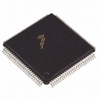
IC DSP 80MHZ 31.5K FLASH 100LQFP
Manufacturer
Freescale Semiconductor
Series
56F8xxr
Datasheet
1.DSP56F826BU80E.pdf
(56 pages)
Specifications of DSP56F826BU80
Core Processor
56800
Core Size
16-Bit
Speed
80MHz
Connectivity
EBI/EMI, SCI, SPI, SSI
Peripherals
POR, WDT
Number Of I /o
46
Program Memory Size
67KB (33.5K x 16)
Program Memory Type
FLASH
Ram Size
4.5K x 16
Voltage - Supply (vcc/vdd)
2.25 V ~ 2.75 V
Oscillator Type
External
Operating Temperature
-40°C ~ 85°C
Package / Case
100-LQFP
Lead Free Status / RoHS Status
Contains lead / RoHS non-compliant
Eeprom Size
-
Data Converters
-
Available stocks
Company
Part Number
Manufacturer
Quantity
Price
Company:

Part Number:
DSP56F826BU80
Manufacturer:
MOTOLOLA
Quantity:
853
Company:
Part Number:
DSP56F826BU80
Manufacturer:
Freescale Semiconductor
Quantity:
10 000
Part Number:
DSP56F826BU80
Manufacturer:
FREESCALE
Quantity:
20 000
Company:
Part Number:
DSP56F826BU80E
Manufacturer:
Freescale Semiconductor
Quantity:
10 000
Part Number:
DSP56F826BU80E
Manufacturer:
FREESCALE
Quantity:
20 000


Part 2 Signal/Connection Descriptions
2.1 Introduction
The input and output signals of the 56F826 are organized into functional groups, as shown in
and as illustrated in
8
Power (V
Ground (V
PLL and Clock
Address Bus
Data Bus
Bus Control
Quad Timer Module Ports
JTAG/On-Chip Emulation (OnCE)
Dedicated General Purpose Input/Output
Synchronous Serial Interface (SSI) Port
Serial Peripheral Interface (SPI) Port
Serial Communications Interface (SCI) Ports
Interrupt and Program Control
Figure
1. Alternately, GPIO pins
Table 2-1 Functional Group Pin Allocations
DD
1
2-1.
SS
, V
, V
1
DDIO or
Table 2-1
SSIO or
Functional Group
V
V
DDA
56F826 Technical Data, Rev. 14
SSA
1
)
)
describes the signal or signals present on a pin.
1
1
Number of Pins
(3,4,1)
(3,4,1)
16
16
16
3
4
4
6
6
4
4
5
Freescale Semiconductor
Table 2-1
Related parts for DSP56F826BU80
Image
Part Number
Description
Manufacturer
Datasheet
Request
R

Part Number:
Description:
Manufacturer:
Freescale Semiconductor, Inc
Datasheet:
Part Number:
Description:
Manufacturer:
Freescale Semiconductor, Inc
Datasheet:
Part Number:
Description:
Manufacturer:
Freescale Semiconductor, Inc
Datasheet:
Part Number:
Description:
Manufacturer:
Freescale Semiconductor, Inc
Datasheet:
Part Number:
Description:
Manufacturer:
Freescale Semiconductor, Inc
Datasheet:
Part Number:
Description:
Manufacturer:
Freescale Semiconductor, Inc
Datasheet:
Part Number:
Description:
Manufacturer:
Freescale Semiconductor, Inc
Datasheet:
Part Number:
Description:
Manufacturer:
Freescale Semiconductor, Inc
Datasheet:
Part Number:
Description:
Manufacturer:
Freescale Semiconductor, Inc
Datasheet:
Part Number:
Description:
Manufacturer:
Freescale Semiconductor, Inc
Datasheet:
Part Number:
Description:
Manufacturer:
Freescale Semiconductor, Inc
Datasheet:
Part Number:
Description:
Manufacturer:
Freescale Semiconductor, Inc
Datasheet:
Part Number:
Description:
Manufacturer:
Freescale Semiconductor, Inc
Datasheet:
Part Number:
Description:
Manufacturer:
Freescale Semiconductor, Inc
Datasheet:
Part Number:
Description:
Manufacturer:
Freescale Semiconductor, Inc
Datasheet: