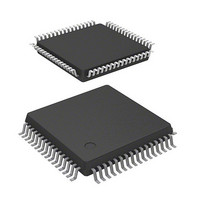
HD64F3684FP Renesas Electronics America, HD64F3684FP Datasheet - Page 245

HD64F3684FP
Manufacturer Part Number
HD64F3684FP
Description
IC H8 MCU FLASH 32K 64LQFP
Manufacturer
Renesas Electronics America
Series
H8® H8/300H Tinyr
Datasheet
1.HD64F3684GFPV.pdf
(538 pages)
Specifications of HD64F3684FP
Core Processor
H8/300H
Core Size
16-Bit
Speed
20MHz
Connectivity
I²C, SCI
Peripherals
PWM, WDT
Number Of I /o
45
Program Memory Size
32KB (32K x 8)
Program Memory Type
FLASH
Ram Size
4K x 8
Voltage - Supply (vcc/vdd)
3 V ~ 5.5 V
Data Converters
A/D 8x10b
Oscillator Type
Internal
Operating Temperature
-20°C ~ 75°C
Package / Case
64-LQFP
Lead Free Status / RoHS Status
Contains lead / RoHS non-compliant
Eeprom Size
-
Available stocks
Company
Part Number
Manufacturer
Quantity
Price
Company:
Part Number:
HD64F3684FPV
Manufacturer:
Renesas Electronics America
Quantity:
10 000
Part Number:
HD64F3684FPV
Manufacturer:
RENESAS/瑞萨
Quantity:
20 000
- Current page: 245 of 538
- Download datasheet (4Mb)
Figure 13.20 shows an example of synchronous operation. In this example, synchronous operation
has been selected, FTIOB0 and FTIOB1 have been designated for PWM mode, GRA_0 compare
match has been set as the channel 0 counter clearing source, and synchronous clearing has been set
for the channel 1 counter clearing source. In addition, the same input clock has been set as the
counter input clock for channel 0 and channel 1. Two-phase PWM waveforms are output from
pins FTIOB0 and FTIOB1. At this time, synchronous presetting and synchronous operation by
GRA_0 compare match are performed by TCNT counters.
For details on PWM mode, see section 13.4.5, PWM Mode.
13.4.5
In PWM mode, PWM waveforms are output from the FTIOB, FTIOC, and FTIOD output pins
with GRA as a cycle register and GRB, GRC, and GRD as duty registers. The initial output level
of the corresponding pin depends on the setting values of TOCR and POCR. Table 13.3 shows an
example of the initial output level of the FTIOB0 pin.
The output level is determined by the POLB to POLD bits corresponding to POCR. When POLB
is 0, the FTIOB output pin is set to 0 by compare match B and set to 1 by compare match A.
When POLB is 1, the FTIOB output pin is set to 1 by compare match B and cleared to 0 by
compare match A. In PWM mode, maximum 6-phase PWM outputs are possible.
Figure 13.21 shows an example of the PWM mode setting procedure.
GRA_0
GRA_1
GRB_0
GRB_1
H'0000
PWM Mode
FTIOB0
FTIOB1
TCNT values
Figure 13.20 Example of Synchronous Operation
Synchronous clearing by GRA_0 compare match
Rev.5.00 Nov. 02, 2005 Page 211 of 500
Section 13 Timer Z
REJ09B0027-0500
Time
Related parts for HD64F3684FP
Image
Part Number
Description
Manufacturer
Datasheet
Request
R

Part Number:
Description:
(HD64 Series) Hitachi Single-Chip Microcomputer
Manufacturer:
Hitachi Semiconductor
Datasheet:

Part Number:
Description:
KIT STARTER FOR M16C/29
Manufacturer:
Renesas Electronics America
Datasheet:

Part Number:
Description:
KIT STARTER FOR R8C/2D
Manufacturer:
Renesas Electronics America
Datasheet:

Part Number:
Description:
R0K33062P STARTER KIT
Manufacturer:
Renesas Electronics America
Datasheet:

Part Number:
Description:
KIT STARTER FOR R8C/23 E8A
Manufacturer:
Renesas Electronics America
Datasheet:

Part Number:
Description:
KIT STARTER FOR R8C/25
Manufacturer:
Renesas Electronics America
Datasheet:

Part Number:
Description:
KIT STARTER H8S2456 SHARPE DSPLY
Manufacturer:
Renesas Electronics America
Datasheet:

Part Number:
Description:
KIT STARTER FOR R8C38C
Manufacturer:
Renesas Electronics America
Datasheet:

Part Number:
Description:
KIT STARTER FOR R8C35C
Manufacturer:
Renesas Electronics America
Datasheet:

Part Number:
Description:
KIT STARTER FOR R8CL3AC+LCD APPS
Manufacturer:
Renesas Electronics America
Datasheet:

Part Number:
Description:
KIT STARTER FOR RX610
Manufacturer:
Renesas Electronics America
Datasheet:

Part Number:
Description:
KIT STARTER FOR R32C/118
Manufacturer:
Renesas Electronics America
Datasheet:

Part Number:
Description:
KIT DEV RSK-R8C/26-29
Manufacturer:
Renesas Electronics America
Datasheet:

Part Number:
Description:
KIT STARTER FOR SH7124
Manufacturer:
Renesas Electronics America
Datasheet:

Part Number:
Description:
KIT STARTER FOR H8SX/1622
Manufacturer:
Renesas Electronics America
Datasheet:


