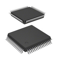
HD64F3684FP Renesas Electronics America, HD64F3684FP Datasheet - Page 256

HD64F3684FP
Manufacturer Part Number
HD64F3684FP
Description
IC H8 MCU FLASH 32K 64LQFP
Manufacturer
Renesas Electronics America
Series
H8® H8/300H Tinyr
Datasheet
1.HD64F3684GFPV.pdf
(538 pages)
Specifications of HD64F3684FP
Core Processor
H8/300H
Core Size
16-Bit
Speed
20MHz
Connectivity
I²C, SCI
Peripherals
PWM, WDT
Number Of I /o
45
Program Memory Size
32KB (32K x 8)
Program Memory Type
FLASH
Ram Size
4K x 8
Voltage - Supply (vcc/vdd)
3 V ~ 5.5 V
Data Converters
A/D 8x10b
Oscillator Type
Internal
Operating Temperature
-20°C ~ 75°C
Package / Case
64-LQFP
Lead Free Status / RoHS Status
Contains lead / RoHS non-compliant
Eeprom Size
-
Available stocks
Company
Part Number
Manufacturer
Quantity
Price
Company:
Part Number:
HD64F3684FPV
Manufacturer:
Renesas Electronics America
Quantity:
10 000
Part Number:
HD64F3684FPV
Manufacturer:
RENESAS/瑞萨
Quantity:
20 000
- Current page: 256 of 538
- Download datasheet (4Mb)
Section 13 Timer Z
Rev.5.00 Nov. 02, 2005 Page 222 of 500
REJ09B0027-0500
Note: To re-enter complementary PWM mode, first, enter a mode other than the complementary
Figure 13.29 Example of Complementar y PWM Mode Setting Procedure
<Complementary PWM mode>
Complementary PWM mode
PWM mode. After that, repeat the setting procedures from step [1].
For settings of waveform outputs with a duty cycle of 0% and 100%, see the settings shown
in 2. Examples of Complementary PWM Mode Operation and 3. Setting GR Value in
Complementary PWM Mode in section 13.4.7.
Enable waveform output
Stop counter operation
Start counter operation
Select counter clock
Initialize output pin
Set complementary
Initialize output pin
PWM mode
Set TCNT
Set GR
[1]
[2]
[3]
[4]
[5]
[6]
[7]
[8]
[9]
[1] Clear bits STR0 and STR1 in TSTR to 0,
[2] Write H'00 to TOCR.
[3] Use bits TPSC2 to TPSC0 in TCR to
[4] Use bits CMD1 and CMD0 in TFCR to set
[5] Set H'00 to TOCR.
[6] TCNT_1 must be H'0000. Set a non-
[7] GRA_0 is a cycle register. Set the cycle to
[8] Use TOER to enable or disable the timer
[9] Set the STR0 and STR1 bits in TSTR to 1
and stop the counter operation of
TCNT_0. Stop TCNT_0 and TCNT_1 and
set complementary PWM mode.
select the same counter clock for channels
0 and 1. When an external clock is
selected, select the edge of the external
clock by bits CKEG1 and CKEG0 in TCR.
Do not use bits CCLR1 and CCLR0 in
TCR to clear the counter.
complementary PWM mode. FTIOB0 to
FTIOD0 and FTIOA1 to FTIOD1
automatically become PWM output pins.
overlapped period to TCNT_0.
GRA_0. Set the timing to change the
PWM output waveform to GRB_0, GRA_1,
and GRB_1. Note that the timing must be
set within the range of compare match
carried out for TCNT_0 and TCNT_1.
For GR settings, see 3. Setting GR Value
in Complementary PWM Mode in section
13.4.7.
output.
to start the count operation.
Related parts for HD64F3684FP
Image
Part Number
Description
Manufacturer
Datasheet
Request
R

Part Number:
Description:
(HD64 Series) Hitachi Single-Chip Microcomputer
Manufacturer:
Hitachi Semiconductor
Datasheet:

Part Number:
Description:
KIT STARTER FOR M16C/29
Manufacturer:
Renesas Electronics America
Datasheet:

Part Number:
Description:
KIT STARTER FOR R8C/2D
Manufacturer:
Renesas Electronics America
Datasheet:

Part Number:
Description:
R0K33062P STARTER KIT
Manufacturer:
Renesas Electronics America
Datasheet:

Part Number:
Description:
KIT STARTER FOR R8C/23 E8A
Manufacturer:
Renesas Electronics America
Datasheet:

Part Number:
Description:
KIT STARTER FOR R8C/25
Manufacturer:
Renesas Electronics America
Datasheet:

Part Number:
Description:
KIT STARTER H8S2456 SHARPE DSPLY
Manufacturer:
Renesas Electronics America
Datasheet:

Part Number:
Description:
KIT STARTER FOR R8C38C
Manufacturer:
Renesas Electronics America
Datasheet:

Part Number:
Description:
KIT STARTER FOR R8C35C
Manufacturer:
Renesas Electronics America
Datasheet:

Part Number:
Description:
KIT STARTER FOR R8CL3AC+LCD APPS
Manufacturer:
Renesas Electronics America
Datasheet:

Part Number:
Description:
KIT STARTER FOR RX610
Manufacturer:
Renesas Electronics America
Datasheet:

Part Number:
Description:
KIT STARTER FOR R32C/118
Manufacturer:
Renesas Electronics America
Datasheet:

Part Number:
Description:
KIT DEV RSK-R8C/26-29
Manufacturer:
Renesas Electronics America
Datasheet:

Part Number:
Description:
KIT STARTER FOR SH7124
Manufacturer:
Renesas Electronics America
Datasheet:

Part Number:
Description:
KIT STARTER FOR H8SX/1622
Manufacturer:
Renesas Electronics America
Datasheet:


