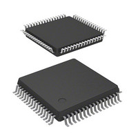
HD64F3684FP Renesas Electronics America, HD64F3684FP Datasheet - Page 283

HD64F3684FP
Manufacturer Part Number
HD64F3684FP
Description
IC H8 MCU FLASH 32K 64LQFP
Manufacturer
Renesas Electronics America
Series
H8® H8/300H Tinyr
Datasheet
1.HD64F3684GFPV.pdf
(538 pages)
Specifications of HD64F3684FP
Core Processor
H8/300H
Core Size
16-Bit
Speed
20MHz
Connectivity
I²C, SCI
Peripherals
PWM, WDT
Number Of I /o
45
Program Memory Size
32KB (32K x 8)
Program Memory Type
FLASH
Ram Size
4K x 8
Voltage - Supply (vcc/vdd)
3 V ~ 5.5 V
Data Converters
A/D 8x10b
Oscillator Type
Internal
Operating Temperature
-20°C ~ 75°C
Package / Case
64-LQFP
Lead Free Status / RoHS Status
Contains lead / RoHS non-compliant
Eeprom Size
-
Available stocks
Company
Part Number
Manufacturer
Quantity
Price
Company:
Part Number:
HD64F3684FPV
Manufacturer:
Renesas Electronics America
Quantity:
10 000
Part Number:
HD64F3684FPV
Manufacturer:
RENESAS/瑞萨
Quantity:
20 000
- Current page: 283 of 538
- Download datasheet (4Mb)
8. Notes on Setting Reset Synchronous PWM Mode/Complementary PWM Mode: When bits
9. Note on Clearing TSR Flag: When a specific flag in TSR is cleared, a combination of the
10. Note on Writing to the TOA0 to TOD0 Bits and the TOA1 to TOD1 Bits in TOCR:
CMD1 and CMD0 in TFCR are set, note the following:
A. Write bits CMD1 and CMD0 while TCNT_1 and TCNT_0 are halted.
B. Changing the settings of reset synchronous PWM mode to complementary PWM mode or
Example: When clearing bit 4 (OVF) in TSR
MOV.B @TSR,R0L
MOV.B #B'11101111, R0L
MOV.B R0L,@TSR
The TOA0 to TOD0 bits and the TOA1 to TOD1 bits in TOCR decide the value of the FTIO
pin, which is output until the first compare match occurs. Once a compare match occurs and
this compare match changes the values of FTIOA0 to FTIOD0 and FTIOA1 to FTIOD1
output, the values of the FTIOA0 to FTIOD0 and FTIOA1 to FTIOD1 pin output and the
values read from the TOA0 to TOD0 and TOA1 to TOD1 bits may differ. Moreover, when the
writing to TOCR and the generation of the compare match A0 to D0 and A1 to D1 occur at the
same timing, the writing to TOCR has the priority. Thus, output change due to the compare
match is not reflected to the FTIOA0 to FTIOD0 and FTIOA1 to FTIOD1 pins. Therefore,
when bit manipulation instruction is used to write to TOCR, the values of the FTIOA0 to
FTIOD0 and FTIOA1 to FTIOD1 pin output may result in an unexpected result. When TOCR
is to be written to while compare match is operating, stop the counter once before accessing to
TOCR, read the port 6 state to reflect the values of FTIOA0 to FTIOD0 and FTIOA1 to
FTIOD1 output, to TOA0 to TOD0 and TOA1 to TOD1, and then restart the counter. Figure
13.59 shows an example when the compare match and the bit manipulation instruction to
TOCR occur at the same timing.
BCLR or MOV instructions is used to read 1 from the flag and then write 0 to the flag.
However, if another bit is set during this processing, the bit may also be cleared
simultaneously. To avoid this, the following processing that does not use the BCLR
instruction must be executed. Note that this note is only applied to the F-ZTAT version. This
problem has already been solved in the mask ROM version.
vice versa is disabled. Set reset synchronous PWM mode or complementary PWM mode
after the normal operation (bits CMD1 and CMD0 are cleared to 0) has been set.
the other bits are all set to 1.
Only the bit to be cleared is 0 and
Rev.5.00 Nov. 02, 2005 Page 249 of 500
Section 13 Timer Z
REJ09B0027-0500
Related parts for HD64F3684FP
Image
Part Number
Description
Manufacturer
Datasheet
Request
R

Part Number:
Description:
(HD64 Series) Hitachi Single-Chip Microcomputer
Manufacturer:
Hitachi Semiconductor
Datasheet:

Part Number:
Description:
KIT STARTER FOR M16C/29
Manufacturer:
Renesas Electronics America
Datasheet:

Part Number:
Description:
KIT STARTER FOR R8C/2D
Manufacturer:
Renesas Electronics America
Datasheet:

Part Number:
Description:
R0K33062P STARTER KIT
Manufacturer:
Renesas Electronics America
Datasheet:

Part Number:
Description:
KIT STARTER FOR R8C/23 E8A
Manufacturer:
Renesas Electronics America
Datasheet:

Part Number:
Description:
KIT STARTER FOR R8C/25
Manufacturer:
Renesas Electronics America
Datasheet:

Part Number:
Description:
KIT STARTER H8S2456 SHARPE DSPLY
Manufacturer:
Renesas Electronics America
Datasheet:

Part Number:
Description:
KIT STARTER FOR R8C38C
Manufacturer:
Renesas Electronics America
Datasheet:

Part Number:
Description:
KIT STARTER FOR R8C35C
Manufacturer:
Renesas Electronics America
Datasheet:

Part Number:
Description:
KIT STARTER FOR R8CL3AC+LCD APPS
Manufacturer:
Renesas Electronics America
Datasheet:

Part Number:
Description:
KIT STARTER FOR RX610
Manufacturer:
Renesas Electronics America
Datasheet:

Part Number:
Description:
KIT STARTER FOR R32C/118
Manufacturer:
Renesas Electronics America
Datasheet:

Part Number:
Description:
KIT DEV RSK-R8C/26-29
Manufacturer:
Renesas Electronics America
Datasheet:

Part Number:
Description:
KIT STARTER FOR SH7124
Manufacturer:
Renesas Electronics America
Datasheet:

Part Number:
Description:
KIT STARTER FOR H8SX/1622
Manufacturer:
Renesas Electronics America
Datasheet:


