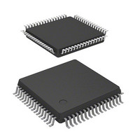
HD64F3684FP Renesas Electronics America, HD64F3684FP Datasheet - Page 293

HD64F3684FP
Manufacturer Part Number
HD64F3684FP
Description
IC H8 MCU FLASH 32K 64LQFP
Manufacturer
Renesas Electronics America
Series
H8® H8/300H Tinyr
Datasheet
1.HD64F3684GFPV.pdf
(538 pages)
Specifications of HD64F3684FP
Core Processor
H8/300H
Core Size
16-Bit
Speed
20MHz
Connectivity
I²C, SCI
Peripherals
PWM, WDT
Number Of I /o
45
Program Memory Size
32KB (32K x 8)
Program Memory Type
FLASH
Ram Size
4K x 8
Voltage - Supply (vcc/vdd)
3 V ~ 5.5 V
Data Converters
A/D 8x10b
Oscillator Type
Internal
Operating Temperature
-20°C ~ 75°C
Package / Case
64-LQFP
Lead Free Status / RoHS Status
Contains lead / RoHS non-compliant
Eeprom Size
-
Available stocks
Company
Part Number
Manufacturer
Quantity
Price
Company:
Part Number:
HD64F3684FPV
Manufacturer:
Renesas Electronics America
Quantity:
10 000
Part Number:
HD64F3684FPV
Manufacturer:
RENESAS/瑞萨
Quantity:
20 000
- Current page: 293 of 538
- Download datasheet (4Mb)
This LSI includes a serial communication interface 3 (SCI3), which has independent two channels.
The SCI3 can handle both asynchronous and clocked synchronous serial communication. In
asynchronous mode, serial data communication can be carried out using standard asynchronous
communication chips such as a Universal Asynchronous Receiver/Transmitter (UART) or an
Asynchronous Communication Interface Adapter (ACIA). A function is also provided for serial
communication between processors (multiprocessor communication function).
Table 16.1 shows the SCI3 channel configuration and figure 16.1 shows a block diagram of the
SCI3. Since pin functions are identical for each of the two channels (SCI3 and SCI3_2), separate
explanations are not given in this section.
16.1
Asynchronous mode
SCI0011A_000020020200
Choice of asynchronous or clocked synchronous serial communication mode
Full-duplex communication capability
The transmitter and receiver are mutually independent, enabling transmission and reception to
be executed simultaneously.
Double-buffering is used in both the transmitter and the receiver, enabling continuous
transmission and continuous reception of serial data.
On-chip baud rate generator allows any bit rate to be selected
External clock or on-chip baud rate generator can be selected as a transfer clock source.
Six interrupt sources
Transmit-end, transmit-data-empty, receive-data-full, overrun error, framing error, and parity
error.
Data length: 7 or 8 bits
Stop bit length: 1 or 2 bits
Parity: Even, odd, or none
Receive error detection: Parity, overrun, and framing errors
Break detection: Break can be detected by reading the RxD pin level directly in the case of a
framing error
Section 16 Serial Communication Interface 3 (SCI3)
Features
Section 16 Serial Communication Interface 3 (SCI3)
Rev.5.00 Nov. 02, 2005 Page 259 of 500
REJ09B0027-0500
Related parts for HD64F3684FP
Image
Part Number
Description
Manufacturer
Datasheet
Request
R

Part Number:
Description:
(HD64 Series) Hitachi Single-Chip Microcomputer
Manufacturer:
Hitachi Semiconductor
Datasheet:

Part Number:
Description:
KIT STARTER FOR M16C/29
Manufacturer:
Renesas Electronics America
Datasheet:

Part Number:
Description:
KIT STARTER FOR R8C/2D
Manufacturer:
Renesas Electronics America
Datasheet:

Part Number:
Description:
R0K33062P STARTER KIT
Manufacturer:
Renesas Electronics America
Datasheet:

Part Number:
Description:
KIT STARTER FOR R8C/23 E8A
Manufacturer:
Renesas Electronics America
Datasheet:

Part Number:
Description:
KIT STARTER FOR R8C/25
Manufacturer:
Renesas Electronics America
Datasheet:

Part Number:
Description:
KIT STARTER H8S2456 SHARPE DSPLY
Manufacturer:
Renesas Electronics America
Datasheet:

Part Number:
Description:
KIT STARTER FOR R8C38C
Manufacturer:
Renesas Electronics America
Datasheet:

Part Number:
Description:
KIT STARTER FOR R8C35C
Manufacturer:
Renesas Electronics America
Datasheet:

Part Number:
Description:
KIT STARTER FOR R8CL3AC+LCD APPS
Manufacturer:
Renesas Electronics America
Datasheet:

Part Number:
Description:
KIT STARTER FOR RX610
Manufacturer:
Renesas Electronics America
Datasheet:

Part Number:
Description:
KIT STARTER FOR R32C/118
Manufacturer:
Renesas Electronics America
Datasheet:

Part Number:
Description:
KIT DEV RSK-R8C/26-29
Manufacturer:
Renesas Electronics America
Datasheet:

Part Number:
Description:
KIT STARTER FOR SH7124
Manufacturer:
Renesas Electronics America
Datasheet:

Part Number:
Description:
KIT STARTER FOR H8SX/1622
Manufacturer:
Renesas Electronics America
Datasheet:


