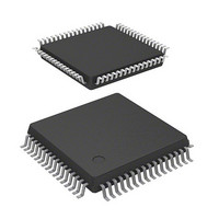
HD64F3684FP Renesas Electronics America, HD64F3684FP Datasheet - Page 388

HD64F3684FP
Manufacturer Part Number
HD64F3684FP
Description
IC H8 MCU FLASH 32K 64LQFP
Manufacturer
Renesas Electronics America
Series
H8® H8/300H Tinyr
Datasheet
1.HD64F3684GFPV.pdf
(538 pages)
Specifications of HD64F3684FP
Core Processor
H8/300H
Core Size
16-Bit
Speed
20MHz
Connectivity
I²C, SCI
Peripherals
PWM, WDT
Number Of I /o
45
Program Memory Size
32KB (32K x 8)
Program Memory Type
FLASH
Ram Size
4K x 8
Voltage - Supply (vcc/vdd)
3 V ~ 5.5 V
Data Converters
A/D 8x10b
Oscillator Type
Internal
Operating Temperature
-20°C ~ 75°C
Package / Case
64-LQFP
Lead Free Status / RoHS Status
Contains lead / RoHS non-compliant
Eeprom Size
-
Available stocks
Company
Part Number
Manufacturer
Quantity
Price
Company:
Part Number:
HD64F3684FPV
Manufacturer:
Renesas Electronics America
Quantity:
10 000
Part Number:
HD64F3684FPV
Manufacturer:
RENESAS/瑞萨
Quantity:
20 000
- Current page: 388 of 538
- Download datasheet (4Mb)
Section 19 EEPROM
The initial value of the slave address code written in the EEPROM is H'00. It can be written in the
range of H'00 to H'07. Be sure to write the data by the byte write method.
The next one bit of the slave address is the R/W code. 0 is for a write and 1 is for a read.
The EEPROM turns to a standby state if the device code is not "1010" or slave address code
doesn’t coincide.
Table 19.2 Slave Addresses
19.4.7
There are two types write operations; byte write operation and page write operation. To initiate
the write operation, input 0 to R/W code following the slave address.
1. Byte Write
Rev.5.00 Nov. 02, 2005 Page 354 of 500
REJ09B0027-0500
Bit
7
6
5
4
3
2
1
A write operation requires an 8-bit data of a 7-bit slave address with R/W code = "0". Then
the EEPROM sends acknowledgement "0" at the ninth bit. This enters the write mode. Then,
two bytes of the memory address are received from the MSB side in the order of upper and
lower. Upon receipt of one-byte memory address, the EEPROM sends acknowledgement "0"
and receives a following a one-byte write data. After receipt of write data, the EEPROM sends
acknowledgement "0". If the EEPROM receives a stop condition, the EEPROM enters an
internally controlled write cycle and terminates receipt of SCL and SDA inputs until
completion of the write cycle. The EEPROM returns to a standby mode after completion of
the write cycle.
The byte write operation is shown in figure 19.3.
Bit name
Device code D3
Device code D2
Device code D1
Device code D0
Slave address code A2
Slave address code A1
Slave address code A0
Write Operations
Initial Value Setting Value Remarks
0
0
0
1
0
1
0
A2
A1
A0
The initial value can be changed
The initial value can be changed
The initial value can be changed
Related parts for HD64F3684FP
Image
Part Number
Description
Manufacturer
Datasheet
Request
R

Part Number:
Description:
(HD64 Series) Hitachi Single-Chip Microcomputer
Manufacturer:
Hitachi Semiconductor
Datasheet:

Part Number:
Description:
KIT STARTER FOR M16C/29
Manufacturer:
Renesas Electronics America
Datasheet:

Part Number:
Description:
KIT STARTER FOR R8C/2D
Manufacturer:
Renesas Electronics America
Datasheet:

Part Number:
Description:
R0K33062P STARTER KIT
Manufacturer:
Renesas Electronics America
Datasheet:

Part Number:
Description:
KIT STARTER FOR R8C/23 E8A
Manufacturer:
Renesas Electronics America
Datasheet:

Part Number:
Description:
KIT STARTER FOR R8C/25
Manufacturer:
Renesas Electronics America
Datasheet:

Part Number:
Description:
KIT STARTER H8S2456 SHARPE DSPLY
Manufacturer:
Renesas Electronics America
Datasheet:

Part Number:
Description:
KIT STARTER FOR R8C38C
Manufacturer:
Renesas Electronics America
Datasheet:

Part Number:
Description:
KIT STARTER FOR R8C35C
Manufacturer:
Renesas Electronics America
Datasheet:

Part Number:
Description:
KIT STARTER FOR R8CL3AC+LCD APPS
Manufacturer:
Renesas Electronics America
Datasheet:

Part Number:
Description:
KIT STARTER FOR RX610
Manufacturer:
Renesas Electronics America
Datasheet:

Part Number:
Description:
KIT STARTER FOR R32C/118
Manufacturer:
Renesas Electronics America
Datasheet:

Part Number:
Description:
KIT DEV RSK-R8C/26-29
Manufacturer:
Renesas Electronics America
Datasheet:

Part Number:
Description:
KIT STARTER FOR SH7124
Manufacturer:
Renesas Electronics America
Datasheet:

Part Number:
Description:
KIT STARTER FOR H8SX/1622
Manufacturer:
Renesas Electronics America
Datasheet:


