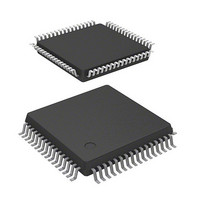
HD64F3684FP Renesas Electronics America, HD64F3684FP Datasheet - Page 390

HD64F3684FP
Manufacturer Part Number
HD64F3684FP
Description
IC H8 MCU FLASH 32K 64LQFP
Manufacturer
Renesas Electronics America
Series
H8® H8/300H Tinyr
Datasheet
1.HD64F3684GFPV.pdf
(538 pages)
Specifications of HD64F3684FP
Core Processor
H8/300H
Core Size
16-Bit
Speed
20MHz
Connectivity
I²C, SCI
Peripherals
PWM, WDT
Number Of I /o
45
Program Memory Size
32KB (32K x 8)
Program Memory Type
FLASH
Ram Size
4K x 8
Voltage - Supply (vcc/vdd)
3 V ~ 5.5 V
Data Converters
A/D 8x10b
Oscillator Type
Internal
Operating Temperature
-20°C ~ 75°C
Package / Case
64-LQFP
Lead Free Status / RoHS Status
Contains lead / RoHS non-compliant
Eeprom Size
-
Available stocks
Company
Part Number
Manufacturer
Quantity
Price
Company:
Part Number:
HD64F3684FPV
Manufacturer:
Renesas Electronics America
Quantity:
10 000
Part Number:
HD64F3684FPV
Manufacturer:
RENESAS/瑞萨
Quantity:
20 000
- Current page: 390 of 538
- Download datasheet (4Mb)
Section 19 EEPROM
19.4.8
Acknowledge polling feature is used to show if the EEPROM is in an internally-timed write cycle
or not. This feature is initiated by the input of the 8-bit slave address + R/W code following the
start condition during an internally-timed write cycle. Acknowledge polling will operate R/W
code = "0". The ninth acknowledgement judges if the EEPROM is an internally-timed write cycle
or not. Acknowledgement "1" shows the EEPROM is in a internally-timed write cycle and
acknowledgement "0" shows the internally-timed write cycle has been completed. The
acknowledge polling starts to function after a write data is input, i.e., when the stop condition is
input.
19.4.9
There are three read operations; current address read, random address read, and sequential read.
Read operations are initiated in the same way as write operations with the exception of R/W = 1.
1. Current Address Read
Rev.5.00 Nov. 02, 2005 Page 356 of 500
REJ09B0027-0500
SCL
SDA
[Legend]
R/W: R/W code (0 is for a write and 1 is for a read),
ACK: acknowledge
The internal address counter maintains the (n+1) address that is made by the last address (n)
accessed during the last read or write operation, with incremented by one. Current address
read accesses the (n+1) address kept by the internal address counter.
After receiving in the order of a start condition and the slave address + R/W code (R/W = 1),
the EEPROM outputs the 1-byte data of the (n+1) address from the most significant bit
following acknowledgement "0". If the EEPROM receives in the order of acknowledgement
"1" and a following stop condition, the EEPROM stops the read operation and is turned to a
standby state.
condition
Start
Acknowledge Polling
Read Operation
1
2
Slave address
3
4
5
6
7
R/W ACK
Figure 19.4 Page Write Operation
8
9
Upper memory
A15
1
address
A8
8
ACK
9
A7
lower memory
1
address
A0
8
ACK
9
D7
1
Write Data
D0
8
ACK
9
D7
Write Data
D0
ACK
conditon
Stop
Related parts for HD64F3684FP
Image
Part Number
Description
Manufacturer
Datasheet
Request
R

Part Number:
Description:
(HD64 Series) Hitachi Single-Chip Microcomputer
Manufacturer:
Hitachi Semiconductor
Datasheet:

Part Number:
Description:
KIT STARTER FOR M16C/29
Manufacturer:
Renesas Electronics America
Datasheet:

Part Number:
Description:
KIT STARTER FOR R8C/2D
Manufacturer:
Renesas Electronics America
Datasheet:

Part Number:
Description:
R0K33062P STARTER KIT
Manufacturer:
Renesas Electronics America
Datasheet:

Part Number:
Description:
KIT STARTER FOR R8C/23 E8A
Manufacturer:
Renesas Electronics America
Datasheet:

Part Number:
Description:
KIT STARTER FOR R8C/25
Manufacturer:
Renesas Electronics America
Datasheet:

Part Number:
Description:
KIT STARTER H8S2456 SHARPE DSPLY
Manufacturer:
Renesas Electronics America
Datasheet:

Part Number:
Description:
KIT STARTER FOR R8C38C
Manufacturer:
Renesas Electronics America
Datasheet:

Part Number:
Description:
KIT STARTER FOR R8C35C
Manufacturer:
Renesas Electronics America
Datasheet:

Part Number:
Description:
KIT STARTER FOR R8CL3AC+LCD APPS
Manufacturer:
Renesas Electronics America
Datasheet:

Part Number:
Description:
KIT STARTER FOR RX610
Manufacturer:
Renesas Electronics America
Datasheet:

Part Number:
Description:
KIT STARTER FOR R32C/118
Manufacturer:
Renesas Electronics America
Datasheet:

Part Number:
Description:
KIT DEV RSK-R8C/26-29
Manufacturer:
Renesas Electronics America
Datasheet:

Part Number:
Description:
KIT STARTER FOR SH7124
Manufacturer:
Renesas Electronics America
Datasheet:

Part Number:
Description:
KIT STARTER FOR H8SX/1622
Manufacturer:
Renesas Electronics America
Datasheet:


