MPC564CVR40 Freescale Semiconductor, MPC564CVR40 Datasheet - Page 831
MPC564CVR40
Manufacturer Part Number
MPC564CVR40
Description
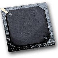
IC MPU 32BIT W/CODE COMP 388PBGA
Manufacturer
Freescale Semiconductor
Series
MPC5xxr
Specifications of MPC564CVR40
Core Processor
PowerPC
Core Size
32-Bit
Speed
40MHz
Connectivity
CAN, EBI/EMI, SCI, SPI, UART/USART
Peripherals
POR, PWM, WDT
Number Of I /o
56
Program Memory Size
512KB (512K x 8)
Program Memory Type
FLASH
Ram Size
32K x 8
Voltage - Supply (vcc/vdd)
2.5 V ~ 2.7 V
Data Converters
A/D 32x10b
Oscillator Type
External
Operating Temperature
-40°C ~ 85°C
Package / Case
388-BGA
Processor Series
MPC5xx
Core
PowerPC
Data Bus Width
32 bit
Data Ram Size
32 KB
Interface Type
CAN, JTAG, QSPI, SCI, SPI, UART
Maximum Clock Frequency
40 MHz
Number Of Programmable I/os
56
Number Of Timers
2
Maximum Operating Temperature
+ 85 C
Mounting Style
SMD/SMT
Minimum Operating Temperature
- 40 C
On-chip Adc
2 (10 bit, 32 Channel)
For Use With
MPC564EVB - KIT EVAL FOR MPC561/562/563/564
Lead Free Status / RoHS Status
Lead free / RoHS Compliant
Eeprom Size
-
Lead Free Status / Rohs Status
Details
Available stocks
Company
Part Number
Manufacturer
Quantity
Price
Company:

Part Number:
MPC564CVR40
Manufacturer:
Freescale Semiconductor
Quantity:
10 000


Chapter 19
Time Processor Unit 3
The time processor unit 3 (TPU3), an enhanced version of the original TPU, is an intelligent,
semi-autonomous microcontroller designed for timing control. The TPU3 is fully compatible to the TPU2.
Operating simultaneously with the CPU, the two TPU3 modules process micro-instructions, schedule and
process real-time hardware events, perform input and output, and access shared data without CPU
intervention. Consequently, for each timer event, the CPU setup and service times are minimized or
eliminated.
The MPC561/MPC563 contains two independent TPU3s: TPU_A and TPU_B. These two TPU3 modules
are memory mapped as shown in
Figure 19-1
Freescale Semiconductor
.
is a simplified block diagram of a single TPU3.
Development
Support and
Parameter
Interface
Channel
Control
System
Config
Host
Test
RAM
DATA
MPC561/MPC563 Reference Manual, Rev. 1.2
Table
TPU_A
TPU_B
Control
TPU
Figure 19-1. TPU3 Block Diagram
Data
Table 19-1. TPU Memory Map
19-1.
Microengine
Scheduler
Execution
Control
Store
Unit
0x30 4000—0x30 43FF
0x30 4400—0x30 47FF
T2CLK
Signal
Address
Control and Data
Service Requests
TCR1
TCR2
Channel 15
Channel 0
Channel 1
Channels
Timer
Pins
19-1
Related parts for MPC564CVR40
Image
Part Number
Description
Manufacturer
Datasheet
Request
R

Part Number:
Description:
MPC5 1K0 5%
Manufacturer:
TE Connectivity
Datasheet:


Part Number:
Description:
MPC5 500R 5%
Manufacturer:
TE Connectivity
Datasheet:

Part Number:
Description:
MPC5 5K0 5%
Manufacturer:
Tyco Electronics
Datasheet:
Part Number:
Description:
MPC5 5R0 5%
Manufacturer:
Tyco Electronics
Datasheet:
Part Number:
Description:
MPC5 50K 5%
Manufacturer:
Tyco Electronics
Datasheet:
Part Number:
Description:
MPC5 1R0 5%
Manufacturer:
Tyco Electronics
Datasheet:

Part Number:
Description:
Manufacturer:
Freescale Semiconductor, Inc
Datasheet:
Part Number:
Description:
Manufacturer:
Freescale Semiconductor, Inc
Datasheet:
Part Number:
Description:
Manufacturer:
Freescale Semiconductor, Inc
Datasheet:
Part Number:
Description:
Manufacturer:
Freescale Semiconductor, Inc
Datasheet:
Part Number:
Description:
Manufacturer:
Freescale Semiconductor, Inc
Datasheet: