R5S72030W200FP Renesas Electronics America, R5S72030W200FP Datasheet - Page 1155
R5S72030W200FP
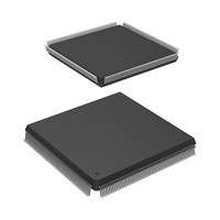
Manufacturer Part Number
R5S72030W200FP
Description
IC SUPERH MPU ROMLESS 240QFP
Manufacturer
Renesas Electronics America
Series
SuperH® SH7200r
Specifications of R5S72030W200FP
Core Processor
SH2A-FPU
Core Size
32-Bit
Speed
200MHz
Connectivity
CAN, I²C, SCI, SSI, SSU, USB
Peripherals
DMA, LCD, POR, PWM, WDT
Number Of I /o
82
Program Memory Type
ROMless
Ram Size
80K x 8
Voltage - Supply (vcc/vdd)
1.1 V ~ 3.6 V
Data Converters
A/D 8x10b; D/A 2x8b
Oscillator Type
Internal
Operating Temperature
-20°C ~ 85°C
Package / Case
240-QFP
For Use With
R0K572030S000BE - KIT DEV FOR SH7203HS0005KCU11H - EMULATOR E10A-USB H8S(X),SH2(A)
Lead Free Status / RoHS Status
Contains lead / RoHS non-compliant
Eeprom Size
-
Program Memory Size
-
Available stocks
Company
Part Number
Manufacturer
Quantity
Price
Company:

Part Number:
R5S72030W200FP
Manufacturer:
SAMSUNG
Quantity:
1 001
Company:
Part Number:
R5S72030W200FP
Manufacturer:
Renesas Electronics America
Quantity:
10 000


23.3.9
CFIFOSIE is a register that controls the SIE functions of the CFIFO port. This register switches
the access right between the SIE and CPU, clears the SIE buffer memory, and checks whether the
SIE buffer is busy or not. This register is not operational when DCP is selected.
This register is initialized by a power-on reset and a software reset.
Initial value:
Bit
15
14
R/W:
Bit:
R/W* R/W*
TGL
FIFO Port SIE Register (CFIFOSIE)
Bit Name
TGL
SCLR
15
0
SCLR SBUSY
14
0
13
R
0
Initial
Value
0
0
12
R
0
-
11
R
0
-
R/W
R/W*
R/W
10
R
0
-
R
9
0
-
Description
Access Right Switch
Sets the buffer memory on the SIE side to the CPU
side. Set the PID bits to NAK and check that the SIE
does not access the buffer memory with the SBUSY
bit (that the SBUSY bit is cleared to 0). Then write
the TGL bit (toggle operation). This bit is valid only
for pipes for which the receiving direction (reading
from the buffer memory) has been set.
0: Invalid
1: Switches the access right
SIE Buffer Clear
Clears the buffer memory on the SIE side. Set the
PID bits to NAK and check that the SIE does not
access the buffer (SBUSY = 0). Then clear the
buffer. This bit is valid only for pipes for which the
transmitting direction (writing to the buffer memory)
has been set.
0: Invalid
1: Clears buffer memory on SIE side
R
8
0
-
Section 23 USB 2.0 Host/Function Module (USB)
R
7
0
-
Rev. 3.00 Sep. 28, 2009 Page 1123 of 1650
R
6
0
-
R
5
0
-
R
4
0
-
R
3
0
-
REJ09B0313-0300
R
2
0
-
R
1
0
-
R
0
0
-
Related parts for R5S72030W200FP
Image
Part Number
Description
Manufacturer
Datasheet
Request
R

Part Number:
Description:
KIT STARTER FOR M16C/29
Manufacturer:
Renesas Electronics America
Datasheet:

Part Number:
Description:
KIT STARTER FOR R8C/2D
Manufacturer:
Renesas Electronics America
Datasheet:

Part Number:
Description:
R0K33062P STARTER KIT
Manufacturer:
Renesas Electronics America
Datasheet:

Part Number:
Description:
KIT STARTER FOR R8C/23 E8A
Manufacturer:
Renesas Electronics America
Datasheet:

Part Number:
Description:
KIT STARTER FOR R8C/25
Manufacturer:
Renesas Electronics America
Datasheet:

Part Number:
Description:
KIT STARTER H8S2456 SHARPE DSPLY
Manufacturer:
Renesas Electronics America
Datasheet:

Part Number:
Description:
KIT STARTER FOR R8C38C
Manufacturer:
Renesas Electronics America
Datasheet:

Part Number:
Description:
KIT STARTER FOR R8C35C
Manufacturer:
Renesas Electronics America
Datasheet:

Part Number:
Description:
KIT STARTER FOR R8CL3AC+LCD APPS
Manufacturer:
Renesas Electronics America
Datasheet:
Part Number:
Description:
KIT STARTER FOR RX610
Manufacturer:
Renesas Electronics America
Datasheet:

Part Number:
Description:
KIT STARTER FOR R32C/118
Manufacturer:
Renesas Electronics America
Datasheet:

Part Number:
Description:
KIT DEV RSK-R8C/26-29
Manufacturer:
Renesas Electronics America
Datasheet:

Part Number:
Description:
KIT STARTER FOR SH7124
Manufacturer:
Renesas Electronics America
Datasheet:

Part Number:
Description:
KIT STARTER FOR H8SX/1622
Manufacturer:
Renesas Electronics America
Datasheet:

Part Number:
Description:
KIT DEV FOR SH7203
Manufacturer:
Renesas Electronics America
Datasheet: