R5S72030W200FP Renesas Electronics America, R5S72030W200FP Datasheet - Page 1393
R5S72030W200FP
Manufacturer Part Number
R5S72030W200FP
Description
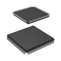
IC SUPERH MPU ROMLESS 240QFP
Manufacturer
Renesas Electronics America
Series
SuperH® SH7200r
Specifications of R5S72030W200FP
Core Processor
SH2A-FPU
Core Size
32-Bit
Speed
200MHz
Connectivity
CAN, I²C, SCI, SSI, SSU, USB
Peripherals
DMA, LCD, POR, PWM, WDT
Number Of I /o
82
Program Memory Type
ROMless
Ram Size
80K x 8
Voltage - Supply (vcc/vdd)
1.1 V ~ 3.6 V
Data Converters
A/D 8x10b; D/A 2x8b
Oscillator Type
Internal
Operating Temperature
-20°C ~ 85°C
Package / Case
240-QFP
For Use With
R0K572030S000BE - KIT DEV FOR SH7203HS0005KCU11H - EMULATOR E10A-USB H8S(X),SH2(A)
Lead Free Status / RoHS Status
Contains lead / RoHS non-compliant
Eeprom Size
-
Program Memory Size
-
Available stocks
Company
Part Number
Manufacturer
Quantity
Price
Company:

Part Number:
R5S72030W200FP
Manufacturer:
SAMSUNG
Quantity:
1 001
Company:
Part Number:
R5S72030W200FP
Manufacturer:
Renesas Electronics America
Quantity:
10 000


25.2.12 SSI Oversampling Clock Selection Register (SCSR)
SCSR is a 16-bit readable/writable register that selects the clock source and division ratio of
oversampling clock used in the SSI.
Initial value:
Bit
15
14 to 12
11
10 to 8
7
6 to 4
3
R/W:
Bit:
Bit Name
⎯
SSI3CKS
[2:0]
⎯
SSI2CKS
[2:0]
⎯
SSI1CKS
[2:0]
⎯
15
R
0
-
R/W
14
0
SSI3CKS[2:0]
R/W
13
0
Initial
Value
0
000
0
000
0
000
0
R/W
12
0
11
R
0
-
R/W
R
R/W
R
R/W
R
R/W
R
R/W
10
0
SSI2CKS[2:0]
R/W
Description
Reserved
This bit is always read as 0. The write value should
always be 0.
SSI ch3 Clock Select
Select the source of the oversampling clock that is
used in channel 3 of the SSI. For settings, see table
25.8.
Reserved
This bit is always read as 0. The write value should
always be 0.
SSI ch2 Clock Select
Select the source of the oversampling clock that is
used in channel 2 of the SSI. For settings, see table
25.8.
Reserved
This bit is always read as 0. The write value should
always be 0.
SSI ch1 Clock Select
Select the source of the oversampling clock that is
used in channel 1 of the SSI. For settings, see table
25.8.
Reserved
This bit is always read as 0. The write value should
always be 0.
9
0
R/W
8
0
R
7
0
-
Rev. 3.00 Sep. 28, 2009 Page 1361 of 1650
R/W
Section 25 Pin Function Controller (PFC)
6
0
SSI1CKS[2:0]
R/W
5
0
R/W
4
0
R
3
0
-
REJ09B0313-0300
R/W
2
0
SSI0CKS[2:0]
R/W
1
0
R/W
0
0
Related parts for R5S72030W200FP
Image
Part Number
Description
Manufacturer
Datasheet
Request
R

Part Number:
Description:
KIT STARTER FOR M16C/29
Manufacturer:
Renesas Electronics America
Datasheet:

Part Number:
Description:
KIT STARTER FOR R8C/2D
Manufacturer:
Renesas Electronics America
Datasheet:

Part Number:
Description:
R0K33062P STARTER KIT
Manufacturer:
Renesas Electronics America
Datasheet:

Part Number:
Description:
KIT STARTER FOR R8C/23 E8A
Manufacturer:
Renesas Electronics America
Datasheet:

Part Number:
Description:
KIT STARTER FOR R8C/25
Manufacturer:
Renesas Electronics America
Datasheet:

Part Number:
Description:
KIT STARTER H8S2456 SHARPE DSPLY
Manufacturer:
Renesas Electronics America
Datasheet:

Part Number:
Description:
KIT STARTER FOR R8C38C
Manufacturer:
Renesas Electronics America
Datasheet:

Part Number:
Description:
KIT STARTER FOR R8C35C
Manufacturer:
Renesas Electronics America
Datasheet:

Part Number:
Description:
KIT STARTER FOR R8CL3AC+LCD APPS
Manufacturer:
Renesas Electronics America
Datasheet:
Part Number:
Description:
KIT STARTER FOR RX610
Manufacturer:
Renesas Electronics America
Datasheet:

Part Number:
Description:
KIT STARTER FOR R32C/118
Manufacturer:
Renesas Electronics America
Datasheet:

Part Number:
Description:
KIT DEV RSK-R8C/26-29
Manufacturer:
Renesas Electronics America
Datasheet:

Part Number:
Description:
KIT STARTER FOR SH7124
Manufacturer:
Renesas Electronics America
Datasheet:

Part Number:
Description:
KIT STARTER FOR H8SX/1622
Manufacturer:
Renesas Electronics America
Datasheet:

Part Number:
Description:
KIT DEV FOR SH7203
Manufacturer:
Renesas Electronics America
Datasheet: