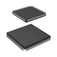
R5S72030W200FP Renesas Electronics America, R5S72030W200FP Datasheet - Page 1444

R5S72030W200FP
Manufacturer Part Number
R5S72030W200FP
Description
IC SUPERH MPU ROMLESS 240QFP
Manufacturer
Renesas Electronics America
Series
SuperH® SH7200r
Specifications of R5S72030W200FP
Core Processor
SH2A-FPU
Core Size
32-Bit
Speed
200MHz
Connectivity
CAN, I²C, SCI, SSI, SSU, USB
Peripherals
DMA, LCD, POR, PWM, WDT
Number Of I /o
82
Program Memory Type
ROMless
Ram Size
80K x 8
Voltage - Supply (vcc/vdd)
1.1 V ~ 3.6 V
Data Converters
A/D 8x10b; D/A 2x8b
Oscillator Type
Internal
Operating Temperature
-20°C ~ 85°C
Package / Case
240-QFP
For Use With
R0K572030S000BE - KIT DEV FOR SH7203HS0005KCU11H - EMULATOR E10A-USB H8S(X),SH2(A)
Lead Free Status / RoHS Status
Contains lead / RoHS non-compliant
Eeprom Size
-
Program Memory Size
-
Available stocks
Company
Part Number
Manufacturer
Quantity
Price
Company:
Part Number:
R5S72030W200FP
Manufacturer:
SAMSUNG
Quantity:
1 001
Company:
Part Number:
R5S72030W200FP
Manufacturer:
Renesas Electronics America
Quantity:
10 000
- Current page: 1444 of 1686
- Download datasheet (10Mb)
Section 28 Power-Down Modes
28.2.8
SYSCR2 is an 8-bit readable/writable register that enables or disables write to the on-chip RAM
(high-speed). Only byte access is valid.
When an RAMWE bit is set to 1, the corresponding on-chip RAM (high-speed) area is enabled.
When an RAMWE bit is cleared to 0, the corresponding on-chip RAM (high-speed) area cannot
be written to. In this case, writing to the on-chip RAM (high-speed) is ignored. The initial value of
an RAMWE bit is 1.
Note that when clearing the RAME bit to 0 to disable the on-chip RAM (high-speed), be sure to
execute an instruction to read from or write to the same arbitrary address in each page before
setting the RAMWE bit. If such an instruction is not executed, the data last written to each page
may not be written to the on-chip RAM (high-speed). Furthermore, an instruction to access the on-
chip RAM (high-speed) should not be located immediately after the instruction to write to
SYSCR2. If an on-chip RAM (high-speed) access instruction is set, normal access is not
guaranteed.
When setting the RAME bit to 1 to enable write to the on-chip RAM (high-speed), an instruction
to read SYSCR2 should be located immediately after the instruction to write to SYSCR2. If an
instruction to access the on-chip RAM (high-speed) is located immediately after the instruction to
write to SYSCR2, normal access is not guaranteed.
Note: When writing to this register, see section 28.4, Usage Notes.
Rev. 3.00 Sep. 28, 2009 Page 1412 of 1650
REJ09B0313-0300
Bit
7 to 4
3
System Control Register 2 (SYSCR2)
Bit Name
⎯
RAMWE3
Initial value:
Initial
Value
All 1
1
R/W:
Bit:
R
7
1
-
R/W
R
R/W
R
6
1
-
Description
Reserved
These bits are always read as 1. The write value
should always be 1.
RAM Write Enable 3 (corresponding area of on-chip
RAM (high-speed): page 3*)
0: Write to on-chip RAM (high-speed) disabled
1: Write to on-chip RAM (high-speed) enabled
R
5
1
-
R
4
1
-
RAM
WE3
R/W
3
1
RAM
WE2
R/W
2
1
RAM
R/W
WE1
1
1
RAM
WE0
R/W
0
1
Related parts for R5S72030W200FP
Image
Part Number
Description
Manufacturer
Datasheet
Request
R

Part Number:
Description:
KIT STARTER FOR M16C/29
Manufacturer:
Renesas Electronics America
Datasheet:

Part Number:
Description:
KIT STARTER FOR R8C/2D
Manufacturer:
Renesas Electronics America
Datasheet:

Part Number:
Description:
R0K33062P STARTER KIT
Manufacturer:
Renesas Electronics America
Datasheet:

Part Number:
Description:
KIT STARTER FOR R8C/23 E8A
Manufacturer:
Renesas Electronics America
Datasheet:

Part Number:
Description:
KIT STARTER FOR R8C/25
Manufacturer:
Renesas Electronics America
Datasheet:

Part Number:
Description:
KIT STARTER H8S2456 SHARPE DSPLY
Manufacturer:
Renesas Electronics America
Datasheet:

Part Number:
Description:
KIT STARTER FOR R8C38C
Manufacturer:
Renesas Electronics America
Datasheet:

Part Number:
Description:
KIT STARTER FOR R8C35C
Manufacturer:
Renesas Electronics America
Datasheet:

Part Number:
Description:
KIT STARTER FOR R8CL3AC+LCD APPS
Manufacturer:
Renesas Electronics America
Datasheet:

Part Number:
Description:
KIT STARTER FOR RX610
Manufacturer:
Renesas Electronics America
Datasheet:

Part Number:
Description:
KIT STARTER FOR R32C/118
Manufacturer:
Renesas Electronics America
Datasheet:

Part Number:
Description:
KIT DEV RSK-R8C/26-29
Manufacturer:
Renesas Electronics America
Datasheet:

Part Number:
Description:
KIT STARTER FOR SH7124
Manufacturer:
Renesas Electronics America
Datasheet:

Part Number:
Description:
KIT STARTER FOR H8SX/1622
Manufacturer:
Renesas Electronics America
Datasheet:

Part Number:
Description:
KIT DEV FOR SH7203
Manufacturer:
Renesas Electronics America
Datasheet:


