R5S72030W200FP Renesas Electronics America, R5S72030W200FP Datasheet - Page 1474
R5S72030W200FP
Manufacturer Part Number
R5S72030W200FP
Description
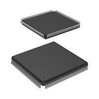
IC SUPERH MPU ROMLESS 240QFP
Manufacturer
Renesas Electronics America
Series
SuperH® SH7200r
Specifications of R5S72030W200FP
Core Processor
SH2A-FPU
Core Size
32-Bit
Speed
200MHz
Connectivity
CAN, I²C, SCI, SSI, SSU, USB
Peripherals
DMA, LCD, POR, PWM, WDT
Number Of I /o
82
Program Memory Type
ROMless
Ram Size
80K x 8
Voltage - Supply (vcc/vdd)
1.1 V ~ 3.6 V
Data Converters
A/D 8x10b; D/A 2x8b
Oscillator Type
Internal
Operating Temperature
-20°C ~ 85°C
Package / Case
240-QFP
For Use With
R0K572030S000BE - KIT DEV FOR SH7203HS0005KCU11H - EMULATOR E10A-USB H8S(X),SH2(A)
Lead Free Status / RoHS Status
Contains lead / RoHS non-compliant
Eeprom Size
-
Program Memory Size
-
Available stocks
Company
Part Number
Manufacturer
Quantity
Price
Company:

Part Number:
R5S72030W200FP
Manufacturer:
SAMSUNG
Quantity:
1 001
Company:
Part Number:
R5S72030W200FP
Manufacturer:
Renesas Electronics America
Quantity:
10 000


Section 29 User Debugging Interface (H-UDI)
29.4.2
Table 29.4 Reset Configuration
Notes: 1. Performs product chip mode and ASE mode settings
29.4.3
The initial value of the TDO change timing is to perform data output from the TDO pin on the
TCK falling edge. However, setting a TDO change timing switch command in SDIR via the H-
UDI pin and passing the Update-IR state synchronizes the TDO change timing to the TCK rising
edge. Hereafter, to synchronize the change timing of TD0 to the falling edge of TCK, the TRST
pin must be simultaneously asserted with the power-on reset. In a case of power-on reset by the
RES pin, the sync reset is still in operation for a certain period in the LSI even after the RES pin is
negated. Thus, if the TRST pin is asserted immediately after the negate of the RES pin, the TD0
change timing switch command is cleared, resulting the TD0 change timing synchronized with the
falling edge of TCK. To prevent this, make sure to put a period of 20 times of tcyc or longer
between the signal change timing of the RES and TRST pins.
Rev. 3.00 Sep. 28, 2009 Page 1442 of 1650
REJ09B0313-0300
ASEMD*
H
L
2. In ASE mode, reset hold is entered if the TRST pin is driven low while the RES pin is
1
Reset Configuration
TDO Output Timing
ASEMD = H, product chip mode
ASEMD = L, ASE mode
negated. In this state, the CPU does not start up. When TRST is driven high, H-UDI
operation is enabled, but the CPU does not start up. The reset hold state is cancelled
by a power-on reset.
RES
L
H
L
H
TRST
L
H
L
H
L
H
L
H
Chip State
Power-on reset and H-UDI reset
Power-on reset
H-UDI reset only
Normal operation
Reset hold*
Power-on reset
H-UDI reset only
Normal operation
2
Related parts for R5S72030W200FP
Image
Part Number
Description
Manufacturer
Datasheet
Request
R

Part Number:
Description:
KIT STARTER FOR M16C/29
Manufacturer:
Renesas Electronics America
Datasheet:

Part Number:
Description:
KIT STARTER FOR R8C/2D
Manufacturer:
Renesas Electronics America
Datasheet:

Part Number:
Description:
R0K33062P STARTER KIT
Manufacturer:
Renesas Electronics America
Datasheet:

Part Number:
Description:
KIT STARTER FOR R8C/23 E8A
Manufacturer:
Renesas Electronics America
Datasheet:

Part Number:
Description:
KIT STARTER FOR R8C/25
Manufacturer:
Renesas Electronics America
Datasheet:

Part Number:
Description:
KIT STARTER H8S2456 SHARPE DSPLY
Manufacturer:
Renesas Electronics America
Datasheet:

Part Number:
Description:
KIT STARTER FOR R8C38C
Manufacturer:
Renesas Electronics America
Datasheet:

Part Number:
Description:
KIT STARTER FOR R8C35C
Manufacturer:
Renesas Electronics America
Datasheet:

Part Number:
Description:
KIT STARTER FOR R8CL3AC+LCD APPS
Manufacturer:
Renesas Electronics America
Datasheet:
Part Number:
Description:
KIT STARTER FOR RX610
Manufacturer:
Renesas Electronics America
Datasheet:

Part Number:
Description:
KIT STARTER FOR R32C/118
Manufacturer:
Renesas Electronics America
Datasheet:

Part Number:
Description:
KIT DEV RSK-R8C/26-29
Manufacturer:
Renesas Electronics America
Datasheet:

Part Number:
Description:
KIT STARTER FOR SH7124
Manufacturer:
Renesas Electronics America
Datasheet:

Part Number:
Description:
KIT STARTER FOR H8SX/1622
Manufacturer:
Renesas Electronics America
Datasheet:

Part Number:
Description:
KIT DEV FOR SH7203
Manufacturer:
Renesas Electronics America
Datasheet: