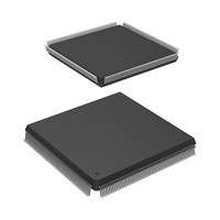
R5S72030W200FP Renesas Electronics America, R5S72030W200FP Datasheet - Page 357

R5S72030W200FP
Manufacturer Part Number
R5S72030W200FP
Description
IC SUPERH MPU ROMLESS 240QFP
Manufacturer
Renesas Electronics America
Series
SuperH® SH7200r
Specifications of R5S72030W200FP
Core Processor
SH2A-FPU
Core Size
32-Bit
Speed
200MHz
Connectivity
CAN, I²C, SCI, SSI, SSU, USB
Peripherals
DMA, LCD, POR, PWM, WDT
Number Of I /o
82
Program Memory Type
ROMless
Ram Size
80K x 8
Voltage - Supply (vcc/vdd)
1.1 V ~ 3.6 V
Data Converters
A/D 8x10b; D/A 2x8b
Oscillator Type
Internal
Operating Temperature
-20°C ~ 85°C
Package / Case
240-QFP
For Use With
R0K572030S000BE - KIT DEV FOR SH7203HS0005KCU11H - EMULATOR E10A-USB H8S(X),SH2(A)
Lead Free Status / RoHS Status
Contains lead / RoHS non-compliant
Eeprom Size
-
Program Memory Size
-
Available stocks
Company
Part Number
Manufacturer
Quantity
Price
Company:
Part Number:
R5S72030W200FP
Manufacturer:
SAMSUNG
Quantity:
1 001
Company:
Part Number:
R5S72030W200FP
Manufacturer:
Renesas Electronics America
Quantity:
10 000
- Current page: 357 of 1686
- Download datasheet (10Mb)
Table 9.13 Relationship between BSZ[1:0], A2/3ROW[1:0], A2/3COL[1:0], and Address
Notes: 1. L/H is a bit used in the command specification; it is fixed at L or H according to the
BSZ
[1:0]
11 (32 bits)
Output Pin of
This LSI
A17
A16
A15
A14
A13
A12
A11
A10
A9
A8
A7
A6
A5
A4
A3
A2
A1
A0
Example of connected memory
512-Mbit product (4 Mwords × 32 bits × 4 banks, column 9 bits product): 1
256-Mbit product (4 Mwords × 16 bits × 4 banks, column 9 bits product): 2
2. Bank address specification
3. Only the RASL pin is asserted because the A 25 pin specified the bank address.
access mode.
RASU is not asserted.
Multiplex Output (3)
A2/3
ROW
[1:0]
10 (13 bits)
Row Address
Output Cycle
A26
A25*
A24*
A23
A22
A21
A20
A19
A18
A17
A16
A15
A14
A13
A12
A11
A10
A9
2
2
*
Setting
3
A2/3
COL
[1:0]
01 (9 bits)
Column Address
Output Cycle
A25*
A24*
A14
A13
L/H*
A11
A10
A9
A8
A7
A6
A5
A4
A3
A2
A1
A0
A17
1
2
2
*
3
SDRAM Pin
A14 (BA1)
A13 (BA0)
A12
A11
A10/AP
A9
A8
A7
A6
A5
A4
A3
A2
A1
A0
Rev. 3.00 Sep. 28, 2009 Page 325 of 1650
Section 9 Bus State Controller (BSC)
Function
Unused
Specifies bank
Address
Specifies
address/precharge
Address
Unused
REJ09B0313-0300
Related parts for R5S72030W200FP
Image
Part Number
Description
Manufacturer
Datasheet
Request
R

Part Number:
Description:
KIT STARTER FOR M16C/29
Manufacturer:
Renesas Electronics America
Datasheet:

Part Number:
Description:
KIT STARTER FOR R8C/2D
Manufacturer:
Renesas Electronics America
Datasheet:

Part Number:
Description:
R0K33062P STARTER KIT
Manufacturer:
Renesas Electronics America
Datasheet:

Part Number:
Description:
KIT STARTER FOR R8C/23 E8A
Manufacturer:
Renesas Electronics America
Datasheet:

Part Number:
Description:
KIT STARTER FOR R8C/25
Manufacturer:
Renesas Electronics America
Datasheet:

Part Number:
Description:
KIT STARTER H8S2456 SHARPE DSPLY
Manufacturer:
Renesas Electronics America
Datasheet:

Part Number:
Description:
KIT STARTER FOR R8C38C
Manufacturer:
Renesas Electronics America
Datasheet:

Part Number:
Description:
KIT STARTER FOR R8C35C
Manufacturer:
Renesas Electronics America
Datasheet:

Part Number:
Description:
KIT STARTER FOR R8CL3AC+LCD APPS
Manufacturer:
Renesas Electronics America
Datasheet:

Part Number:
Description:
KIT STARTER FOR RX610
Manufacturer:
Renesas Electronics America
Datasheet:

Part Number:
Description:
KIT STARTER FOR R32C/118
Manufacturer:
Renesas Electronics America
Datasheet:

Part Number:
Description:
KIT DEV RSK-R8C/26-29
Manufacturer:
Renesas Electronics America
Datasheet:

Part Number:
Description:
KIT STARTER FOR SH7124
Manufacturer:
Renesas Electronics America
Datasheet:

Part Number:
Description:
KIT STARTER FOR H8SX/1622
Manufacturer:
Renesas Electronics America
Datasheet:

Part Number:
Description:
KIT DEV FOR SH7203
Manufacturer:
Renesas Electronics America
Datasheet:


