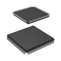
R5S72030W200FP Renesas Electronics America, R5S72030W200FP Datasheet - Page 369

R5S72030W200FP
Manufacturer Part Number
R5S72030W200FP
Description
IC SUPERH MPU ROMLESS 240QFP
Manufacturer
Renesas Electronics America
Series
SuperH® SH7200r
Specifications of R5S72030W200FP
Core Processor
SH2A-FPU
Core Size
32-Bit
Speed
200MHz
Connectivity
CAN, I²C, SCI, SSI, SSU, USB
Peripherals
DMA, LCD, POR, PWM, WDT
Number Of I /o
82
Program Memory Type
ROMless
Ram Size
80K x 8
Voltage - Supply (vcc/vdd)
1.1 V ~ 3.6 V
Data Converters
A/D 8x10b; D/A 2x8b
Oscillator Type
Internal
Operating Temperature
-20°C ~ 85°C
Package / Case
240-QFP
For Use With
R0K572030S000BE - KIT DEV FOR SH7203HS0005KCU11H - EMULATOR E10A-USB H8S(X),SH2(A)
Lead Free Status / RoHS Status
Contains lead / RoHS non-compliant
Eeprom Size
-
Program Memory Size
-
Available stocks
Company
Part Number
Manufacturer
Quantity
Price
Company:
Part Number:
R5S72030W200FP
Manufacturer:
SAMSUNG
Quantity:
1 001
Company:
Part Number:
R5S72030W200FP
Manufacturer:
Renesas Electronics America
Quantity:
10 000
- Current page: 369 of 1686
- Download datasheet (10Mb)
Section 9 Bus State Controller (BSC)
(5)
Burst Write
A burst write occurs in the following cases in this LSI.
• Access size in writing is larger than data bus width.
• Write-back of the cache
• 16-byte transfer in DMAC
This LSI always accesses SDRAM with burst length 1. For example, write access of burst length 1
is performed continuously 4 times to write 16-byte continuous data to the SDRAM that is
connected to a 32-bit data bus. This access is called burst write with the burst number 4. The
relationship between the access size and the number of bursts is shown in table 9.17. Figure 9.20
shows a timing chart for burst writes. In burst write, an ACTV command is output in the Tr cycle,
the WRIT command is issued in the Tc1, Tc2, and Tc3 cycles, and the WRITA command is issued
to execute an auto-precharge in the Tc4 cycle. In the write cycle, the write data is output
simultaneously with the write command. After the write command with the auto-precharge is
output, the Trw1 cycle that waits for the auto-precharge initiation is followed by the Tap cycle that
waits for completion of the auto-precharge induced by the WRITA command in the SDRAM.
Between the Trwl and the Tap cycle, a new command will not be issued to the same bank.
However, access to another CS space or another bank in the same SDRAM space is enabled. The
number of Trw1 cycles is specified by the TRWL1 and TRWL0 bits in CS3WCR. The number of
Tap cycles is specified by the WTRP1 and WTRP0 bits in CS3WCR.
Rev. 3.00 Sep. 28, 2009 Page 337 of 1650
REJ09B0313-0300
Related parts for R5S72030W200FP
Image
Part Number
Description
Manufacturer
Datasheet
Request
R

Part Number:
Description:
KIT STARTER FOR M16C/29
Manufacturer:
Renesas Electronics America
Datasheet:

Part Number:
Description:
KIT STARTER FOR R8C/2D
Manufacturer:
Renesas Electronics America
Datasheet:

Part Number:
Description:
R0K33062P STARTER KIT
Manufacturer:
Renesas Electronics America
Datasheet:

Part Number:
Description:
KIT STARTER FOR R8C/23 E8A
Manufacturer:
Renesas Electronics America
Datasheet:

Part Number:
Description:
KIT STARTER FOR R8C/25
Manufacturer:
Renesas Electronics America
Datasheet:

Part Number:
Description:
KIT STARTER H8S2456 SHARPE DSPLY
Manufacturer:
Renesas Electronics America
Datasheet:

Part Number:
Description:
KIT STARTER FOR R8C38C
Manufacturer:
Renesas Electronics America
Datasheet:

Part Number:
Description:
KIT STARTER FOR R8C35C
Manufacturer:
Renesas Electronics America
Datasheet:

Part Number:
Description:
KIT STARTER FOR R8CL3AC+LCD APPS
Manufacturer:
Renesas Electronics America
Datasheet:

Part Number:
Description:
KIT STARTER FOR RX610
Manufacturer:
Renesas Electronics America
Datasheet:

Part Number:
Description:
KIT STARTER FOR R32C/118
Manufacturer:
Renesas Electronics America
Datasheet:

Part Number:
Description:
KIT DEV RSK-R8C/26-29
Manufacturer:
Renesas Electronics America
Datasheet:

Part Number:
Description:
KIT STARTER FOR SH7124
Manufacturer:
Renesas Electronics America
Datasheet:

Part Number:
Description:
KIT STARTER FOR H8SX/1622
Manufacturer:
Renesas Electronics America
Datasheet:

Part Number:
Description:
KIT DEV FOR SH7203
Manufacturer:
Renesas Electronics America
Datasheet:


