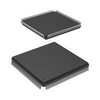
R5S72030W200FP Renesas Electronics America, R5S72030W200FP Datasheet - Page 373

R5S72030W200FP
Manufacturer Part Number
R5S72030W200FP
Description
IC SUPERH MPU ROMLESS 240QFP
Manufacturer
Renesas Electronics America
Series
SuperH® SH7200r
Specifications of R5S72030W200FP
Core Processor
SH2A-FPU
Core Size
32-Bit
Speed
200MHz
Connectivity
CAN, I²C, SCI, SSI, SSU, USB
Peripherals
DMA, LCD, POR, PWM, WDT
Number Of I /o
82
Program Memory Type
ROMless
Ram Size
80K x 8
Voltage - Supply (vcc/vdd)
1.1 V ~ 3.6 V
Data Converters
A/D 8x10b; D/A 2x8b
Oscillator Type
Internal
Operating Temperature
-20°C ~ 85°C
Package / Case
240-QFP
For Use With
R0K572030S000BE - KIT DEV FOR SH7203HS0005KCU11H - EMULATOR E10A-USB H8S(X),SH2(A)
Lead Free Status / RoHS Status
Contains lead / RoHS non-compliant
Eeprom Size
-
Program Memory Size
-
Available stocks
Company
Part Number
Manufacturer
Quantity
Price
Company:
Part Number:
R5S72030W200FP
Manufacturer:
SAMSUNG
Quantity:
1 001
Company:
Part Number:
R5S72030W200FP
Manufacturer:
Renesas Electronics America
Quantity:
10 000
- Current page: 373 of 1686
- Download datasheet (10Mb)
latency is specified as two cycles or more, the Tnop cycle is not inserted because the two cycles of
latency can be acquired even if the DQMxx signal is asserted after the Tc cycle.
When bank active mode is set, if only access cycles to the respective banks in the area 3 space are
considered, as long as access cycles to the same row address continue, the operation starts with the
cycle in figure 9.22 or 9.25, followed by repetition of the cycle in figure 9.23 or 9.26. An access to
a different area during this time has no effect. If there is an access to a different row address in the
bank active state, the bus cycle in figure 9.24 or 9.27 is executed instead of that in figure 9.23 or
9.26. In bank active mode, too, all banks become inactive after a refresh cycle or after the bus is
released as the result of bus arbitration.
Figure 9.22 Burst Read Timing (Bank Active, Different Bank, CAS Latency 1)
RASL, RASU
CASL, CASU
Notes: 1. Address pin to be connected to pin A10 of SDRAM.
A12/A11*
D31 to D0
A25 to A0
DACKn*
RD/WR
DQMxx
CKIO
2. The waveform for DACKn is when active low is specified.
CS3
BS
1
2
Tr
Tc1
Td1
Tc2
Td2
Tc3
Rev. 3.00 Sep. 28, 2009 Page 341 of 1650
Td3
Tc4
Section 9 Bus State Controller (BSC)
Td4
Tde
REJ09B0313-0300
Related parts for R5S72030W200FP
Image
Part Number
Description
Manufacturer
Datasheet
Request
R

Part Number:
Description:
KIT STARTER FOR M16C/29
Manufacturer:
Renesas Electronics America
Datasheet:

Part Number:
Description:
KIT STARTER FOR R8C/2D
Manufacturer:
Renesas Electronics America
Datasheet:

Part Number:
Description:
R0K33062P STARTER KIT
Manufacturer:
Renesas Electronics America
Datasheet:

Part Number:
Description:
KIT STARTER FOR R8C/23 E8A
Manufacturer:
Renesas Electronics America
Datasheet:

Part Number:
Description:
KIT STARTER FOR R8C/25
Manufacturer:
Renesas Electronics America
Datasheet:

Part Number:
Description:
KIT STARTER H8S2456 SHARPE DSPLY
Manufacturer:
Renesas Electronics America
Datasheet:

Part Number:
Description:
KIT STARTER FOR R8C38C
Manufacturer:
Renesas Electronics America
Datasheet:

Part Number:
Description:
KIT STARTER FOR R8C35C
Manufacturer:
Renesas Electronics America
Datasheet:

Part Number:
Description:
KIT STARTER FOR R8CL3AC+LCD APPS
Manufacturer:
Renesas Electronics America
Datasheet:

Part Number:
Description:
KIT STARTER FOR RX610
Manufacturer:
Renesas Electronics America
Datasheet:

Part Number:
Description:
KIT STARTER FOR R32C/118
Manufacturer:
Renesas Electronics America
Datasheet:

Part Number:
Description:
KIT DEV RSK-R8C/26-29
Manufacturer:
Renesas Electronics America
Datasheet:

Part Number:
Description:
KIT STARTER FOR SH7124
Manufacturer:
Renesas Electronics America
Datasheet:

Part Number:
Description:
KIT STARTER FOR H8SX/1622
Manufacturer:
Renesas Electronics America
Datasheet:

Part Number:
Description:
KIT DEV FOR SH7203
Manufacturer:
Renesas Electronics America
Datasheet:


