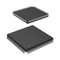
R5S72030W200FP Renesas Electronics America, R5S72030W200FP Datasheet - Page 422

R5S72030W200FP
Manufacturer Part Number
R5S72030W200FP
Description
IC SUPERH MPU ROMLESS 240QFP
Manufacturer
Renesas Electronics America
Series
SuperH® SH7200r
Specifications of R5S72030W200FP
Core Processor
SH2A-FPU
Core Size
32-Bit
Speed
200MHz
Connectivity
CAN, I²C, SCI, SSI, SSU, USB
Peripherals
DMA, LCD, POR, PWM, WDT
Number Of I /o
82
Program Memory Type
ROMless
Ram Size
80K x 8
Voltage - Supply (vcc/vdd)
1.1 V ~ 3.6 V
Data Converters
A/D 8x10b; D/A 2x8b
Oscillator Type
Internal
Operating Temperature
-20°C ~ 85°C
Package / Case
240-QFP
For Use With
R0K572030S000BE - KIT DEV FOR SH7203HS0005KCU11H - EMULATOR E10A-USB H8S(X),SH2(A)
Lead Free Status / RoHS Status
Contains lead / RoHS non-compliant
Eeprom Size
-
Program Memory Size
-
Available stocks
Company
Part Number
Manufacturer
Quantity
Price
Company:
Part Number:
R5S72030W200FP
Manufacturer:
SAMSUNG
Quantity:
1 001
Company:
Part Number:
R5S72030W200FP
Manufacturer:
Renesas Electronics America
Quantity:
10 000
- Current page: 422 of 1686
- Download datasheet (10Mb)
Section 9 Bus State Controller (BSC)
CPU performs four contiguous longword read cycles to perform cache fill operations via the
internal bus. If a cache miss occurs in byte or word operand access or at a branch to an odd word
boundary (4n + 2), the CPU performs four contiguous longword access cycles to perform a cache
fill operation on the external interface. For a cache-disabled space, the CPU performs access
according to the actual access addresses. For an instruction fetch to an even word boundary (4n),
the CPU performs longword access. For an instruction fetch to an odd word boundary (4n + 2), the
CPU performs word access.
For a read cycle of an on-chip peripheral module, the cycle is initiated through the internal bus and
peripheral bus. The read data is sent to the CPU via the peripheral bus, internal bus, and CPU bus.
In a write cycle for the cache-enabled space, the write cycle operation differs according to the
cache write methods.
In write-back mode, the cache is first searched. If data is detected at the address corresponding to
the cache, the data is then re-written to the cache. In the actual memory, data will not be re-written
until data in the corresponding address is re-written. If data is not detected at the address
corresponding to the cache, the cache is modified. In this case, data to be modified is first saved to
the internal buffer, 16-byte data including the data corresponding to the address is then read, and
data in the corresponding access of the cache is finally modified. Following these operations, a
write-back cycle for the saved 16-byte data is executed.
In write-through mode, the cache is first searched. If data is detected at the address corresponding
to the cache, the data is re-written to the cache simultaneously with the actual write via the internal
bus. If data is not detected at the address corresponding to the cache, the cache is not modified but
an actual write is performed via the internal bus.
Since the bus state controller (BSC) incorporates a one-stage write buffer, the BSC can execute an
access via the internal bus before the previous external bus cycle is completed in a write cycle. If
the on-chip module is read or written after the external low-speed memory is written, the on-chip
module can be accessed before the completion of the external low-speed memory write cycle.
In read cycles, the CPU is placed in the wait state until read operation has been completed. To
continue the process after the data write to the device has been completed, perform a dummy read
to the same address to check for completion of the write before the next process to be executed.
The write buffer of the BSC functions in the same way for an access by a bus master other than
the CPU such as the DMAC. Accordingly, to perform dual address DMA transfers, the next read
cycle is initiated before the previous write cycle is completed. Note, however, that if both the
DMA source and destination addresses exist in external memory space, the next write cycle will
not be initiated until the previous write cycle is completed.
Rev. 3.00 Sep. 28, 2009 Page 390 of 1650
REJ09B0313-0300
Related parts for R5S72030W200FP
Image
Part Number
Description
Manufacturer
Datasheet
Request
R

Part Number:
Description:
KIT STARTER FOR M16C/29
Manufacturer:
Renesas Electronics America
Datasheet:

Part Number:
Description:
KIT STARTER FOR R8C/2D
Manufacturer:
Renesas Electronics America
Datasheet:

Part Number:
Description:
R0K33062P STARTER KIT
Manufacturer:
Renesas Electronics America
Datasheet:

Part Number:
Description:
KIT STARTER FOR R8C/23 E8A
Manufacturer:
Renesas Electronics America
Datasheet:

Part Number:
Description:
KIT STARTER FOR R8C/25
Manufacturer:
Renesas Electronics America
Datasheet:

Part Number:
Description:
KIT STARTER H8S2456 SHARPE DSPLY
Manufacturer:
Renesas Electronics America
Datasheet:

Part Number:
Description:
KIT STARTER FOR R8C38C
Manufacturer:
Renesas Electronics America
Datasheet:

Part Number:
Description:
KIT STARTER FOR R8C35C
Manufacturer:
Renesas Electronics America
Datasheet:

Part Number:
Description:
KIT STARTER FOR R8CL3AC+LCD APPS
Manufacturer:
Renesas Electronics America
Datasheet:

Part Number:
Description:
KIT STARTER FOR RX610
Manufacturer:
Renesas Electronics America
Datasheet:

Part Number:
Description:
KIT STARTER FOR R32C/118
Manufacturer:
Renesas Electronics America
Datasheet:

Part Number:
Description:
KIT DEV RSK-R8C/26-29
Manufacturer:
Renesas Electronics America
Datasheet:

Part Number:
Description:
KIT STARTER FOR SH7124
Manufacturer:
Renesas Electronics America
Datasheet:

Part Number:
Description:
KIT STARTER FOR H8SX/1622
Manufacturer:
Renesas Electronics America
Datasheet:

Part Number:
Description:
KIT DEV FOR SH7203
Manufacturer:
Renesas Electronics America
Datasheet:


