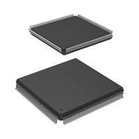
R5S72030W200FP Renesas Electronics America, R5S72030W200FP Datasheet - Page 566

R5S72030W200FP
Manufacturer Part Number
R5S72030W200FP
Description
IC SUPERH MPU ROMLESS 240QFP
Manufacturer
Renesas Electronics America
Series
SuperH® SH7200r
Specifications of R5S72030W200FP
Core Processor
SH2A-FPU
Core Size
32-Bit
Speed
200MHz
Connectivity
CAN, I²C, SCI, SSI, SSU, USB
Peripherals
DMA, LCD, POR, PWM, WDT
Number Of I /o
82
Program Memory Type
ROMless
Ram Size
80K x 8
Voltage - Supply (vcc/vdd)
1.1 V ~ 3.6 V
Data Converters
A/D 8x10b; D/A 2x8b
Oscillator Type
Internal
Operating Temperature
-20°C ~ 85°C
Package / Case
240-QFP
For Use With
R0K572030S000BE - KIT DEV FOR SH7203HS0005KCU11H - EMULATOR E10A-USB H8S(X),SH2(A)
Lead Free Status / RoHS Status
Contains lead / RoHS non-compliant
Eeprom Size
-
Program Memory Size
-
Available stocks
Company
Part Number
Manufacturer
Quantity
Price
Company:
Part Number:
R5S72030W200FP
Manufacturer:
SAMSUNG
Quantity:
1 001
Company:
Part Number:
R5S72030W200FP
Manufacturer:
Renesas Electronics America
Quantity:
10 000
- Current page: 566 of 1686
- Download datasheet (10Mb)
Section 11 Multi-Function Timer Pulse Unit 2 (MTU2)
(3)
The timing for transfer from buffer registers to timer general registers can be selected in PWM
mode 1 or 2 for channel 0 or in PWM mode 1 for channels 3 and 4 by setting the buffer operation
transfer mode registers (TBTM_0, TBTM_3, and TBTM_4). Either compare match (initial
setting) or TCNT clearing can be selected for the transfer timing. TCNT clearing as transfer
timing is one of the following cases.
• When TCNT overflows (H'FFFF to H'0000)
• When H'0000 is written to TCNT during counting
• When TCNT is cleared to H'0000 under the condition specified in the CCLR2 to CCLR0 bits
Note: TBTM must be modified only while TCNT stops.
Figure 11.19 shows an operation example in which PWM mode 1 is designated for channel 0 and
buffer operation is designated for TGRA_0 and TGRC_0. The settings used in this example are
TCNT_0 clearing by compare match B, 1 output at compare match A, and 0 output at compare
match B. The TTSA bit in TBTM_0 is set to 1.
Rev. 3.00 Sep. 28, 2009 Page 534 of 1650
REJ09B0313-0300
in TCR
Selecting Timing for Transfer from Buffer Registers to Timer General Registers in
Buffer Operation
H'0F07
H'09FB
H'0532
H'0000
TIOCA
TGRA
TGRC
TCNT value
Figure 11.18 Example of Buffer Operation (2)
H'0532
H'0F07
H'0532
H'09FB
H'0F07
Time
Related parts for R5S72030W200FP
Image
Part Number
Description
Manufacturer
Datasheet
Request
R

Part Number:
Description:
KIT STARTER FOR M16C/29
Manufacturer:
Renesas Electronics America
Datasheet:

Part Number:
Description:
KIT STARTER FOR R8C/2D
Manufacturer:
Renesas Electronics America
Datasheet:

Part Number:
Description:
R0K33062P STARTER KIT
Manufacturer:
Renesas Electronics America
Datasheet:

Part Number:
Description:
KIT STARTER FOR R8C/23 E8A
Manufacturer:
Renesas Electronics America
Datasheet:

Part Number:
Description:
KIT STARTER FOR R8C/25
Manufacturer:
Renesas Electronics America
Datasheet:

Part Number:
Description:
KIT STARTER H8S2456 SHARPE DSPLY
Manufacturer:
Renesas Electronics America
Datasheet:

Part Number:
Description:
KIT STARTER FOR R8C38C
Manufacturer:
Renesas Electronics America
Datasheet:

Part Number:
Description:
KIT STARTER FOR R8C35C
Manufacturer:
Renesas Electronics America
Datasheet:

Part Number:
Description:
KIT STARTER FOR R8CL3AC+LCD APPS
Manufacturer:
Renesas Electronics America
Datasheet:

Part Number:
Description:
KIT STARTER FOR RX610
Manufacturer:
Renesas Electronics America
Datasheet:

Part Number:
Description:
KIT STARTER FOR R32C/118
Manufacturer:
Renesas Electronics America
Datasheet:

Part Number:
Description:
KIT DEV RSK-R8C/26-29
Manufacturer:
Renesas Electronics America
Datasheet:

Part Number:
Description:
KIT STARTER FOR SH7124
Manufacturer:
Renesas Electronics America
Datasheet:

Part Number:
Description:
KIT STARTER FOR H8SX/1622
Manufacturer:
Renesas Electronics America
Datasheet:

Part Number:
Description:
KIT DEV FOR SH7203
Manufacturer:
Renesas Electronics America
Datasheet:


