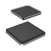
R5S72030W200FP Renesas Electronics America, R5S72030W200FP Datasheet - Page 840

R5S72030W200FP
Manufacturer Part Number
R5S72030W200FP
Description
IC SUPERH MPU ROMLESS 240QFP
Manufacturer
Renesas Electronics America
Series
SuperH® SH7200r
Specifications of R5S72030W200FP
Core Processor
SH2A-FPU
Core Size
32-Bit
Speed
200MHz
Connectivity
CAN, I²C, SCI, SSI, SSU, USB
Peripherals
DMA, LCD, POR, PWM, WDT
Number Of I /o
82
Program Memory Type
ROMless
Ram Size
80K x 8
Voltage - Supply (vcc/vdd)
1.1 V ~ 3.6 V
Data Converters
A/D 8x10b; D/A 2x8b
Oscillator Type
Internal
Operating Temperature
-20°C ~ 85°C
Package / Case
240-QFP
For Use With
R0K572030S000BE - KIT DEV FOR SH7203HS0005KCU11H - EMULATOR E10A-USB H8S(X),SH2(A)
Lead Free Status / RoHS Status
Contains lead / RoHS non-compliant
Eeprom Size
-
Program Memory Size
-
Available stocks
Company
Part Number
Manufacturer
Quantity
Price
Company:
Part Number:
R5S72030W200FP
Manufacturer:
SAMSUNG
Quantity:
1 001
Company:
Part Number:
R5S72030W200FP
Manufacturer:
Renesas Electronics America
Quantity:
10 000
- Current page: 840 of 1686
- Download datasheet (10Mb)
Section 16 Synchronous Serial Communication Unit (SSU)
16.4
16.4.1
A transfer clock can be selected from among seven internal clocks and an external clock. Before
using this module, enable the SSCK pin function in the PFC. When the MSS bit in SSCRH is 1, an
internal clock is selected and the SSCK pin is used as an output pin. When transfer is started, the
clock with the transfer rate set by bits CKS2 to CKS0 in SSMR is output from the SSCK pin.
When MSS = 0, an external clock is selected and the SSCK pin is used as an input pin.
16.4.2
The relationship of clock phase, polarity, and transfer data depends on the combination of the
CPOS and CPHS bits in SSMR when the value of the SSUMS bit in SSCRL is 0. Figure 16.2
shows the relationship. When SSUMS = 1, the CPHS setting is invalid although the CPOS setting
is valid. When SSUMS = 1, the transmit data change timing and receive data fetch timing are the
same as that shown as “(1) When CPHS = 0” in figure 16.2.
Setting the MLS bit in SSMR selects either MSB first or LSB first communication. When MLS =
0, data is transferred from the LSB to the MSB. When MLS = 1, data is transferred from the MSB
to the LSB.
Rev. 3.00 Sep. 28, 2009 Page 808 of 1650
REJ09B0313-0300
(1) When CPHS = 0
(2) When CPHS = 1
(CPOS = 0)
(CPOS = 1)
(CPOS = 0)
(CPOS = 1)
SSI, SSO
SSI, SSO
Operation
Transfer Clock
Relationship of Clock Phase, Polarity, and Data
SSCK
SSCK
SSCK
SSCK
SCS
SCS
Figure 16.2 Relationship of Clock Phase, Polarity, and Data
Bit 0
Bit 0
Bit 1
Bit 1
Bit 2
Bit 2
Bit 3
Bit 3
Bit 4
Bit 4
Bit 5
Bit 5
Bit 6
Bit 6
Bit 7
Bit 7
Related parts for R5S72030W200FP
Image
Part Number
Description
Manufacturer
Datasheet
Request
R

Part Number:
Description:
KIT STARTER FOR M16C/29
Manufacturer:
Renesas Electronics America
Datasheet:

Part Number:
Description:
KIT STARTER FOR R8C/2D
Manufacturer:
Renesas Electronics America
Datasheet:

Part Number:
Description:
R0K33062P STARTER KIT
Manufacturer:
Renesas Electronics America
Datasheet:

Part Number:
Description:
KIT STARTER FOR R8C/23 E8A
Manufacturer:
Renesas Electronics America
Datasheet:

Part Number:
Description:
KIT STARTER FOR R8C/25
Manufacturer:
Renesas Electronics America
Datasheet:

Part Number:
Description:
KIT STARTER H8S2456 SHARPE DSPLY
Manufacturer:
Renesas Electronics America
Datasheet:

Part Number:
Description:
KIT STARTER FOR R8C38C
Manufacturer:
Renesas Electronics America
Datasheet:

Part Number:
Description:
KIT STARTER FOR R8C35C
Manufacturer:
Renesas Electronics America
Datasheet:

Part Number:
Description:
KIT STARTER FOR R8CL3AC+LCD APPS
Manufacturer:
Renesas Electronics America
Datasheet:

Part Number:
Description:
KIT STARTER FOR RX610
Manufacturer:
Renesas Electronics America
Datasheet:

Part Number:
Description:
KIT STARTER FOR R32C/118
Manufacturer:
Renesas Electronics America
Datasheet:

Part Number:
Description:
KIT DEV RSK-R8C/26-29
Manufacturer:
Renesas Electronics America
Datasheet:

Part Number:
Description:
KIT STARTER FOR SH7124
Manufacturer:
Renesas Electronics America
Datasheet:

Part Number:
Description:
KIT STARTER FOR H8SX/1622
Manufacturer:
Renesas Electronics America
Datasheet:

Part Number:
Description:
KIT DEV FOR SH7203
Manufacturer:
Renesas Electronics America
Datasheet:


