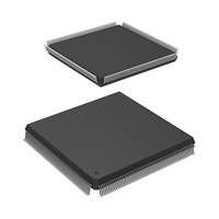
R5S72030W200FP Renesas Electronics America, R5S72030W200FP Datasheet - Page 841

R5S72030W200FP
Manufacturer Part Number
R5S72030W200FP
Description
IC SUPERH MPU ROMLESS 240QFP
Manufacturer
Renesas Electronics America
Series
SuperH® SH7200r
Specifications of R5S72030W200FP
Core Processor
SH2A-FPU
Core Size
32-Bit
Speed
200MHz
Connectivity
CAN, I²C, SCI, SSI, SSU, USB
Peripherals
DMA, LCD, POR, PWM, WDT
Number Of I /o
82
Program Memory Type
ROMless
Ram Size
80K x 8
Voltage - Supply (vcc/vdd)
1.1 V ~ 3.6 V
Data Converters
A/D 8x10b; D/A 2x8b
Oscillator Type
Internal
Operating Temperature
-20°C ~ 85°C
Package / Case
240-QFP
For Use With
R0K572030S000BE - KIT DEV FOR SH7203HS0005KCU11H - EMULATOR E10A-USB H8S(X),SH2(A)
Lead Free Status / RoHS Status
Contains lead / RoHS non-compliant
Eeprom Size
-
Program Memory Size
-
Available stocks
Company
Part Number
Manufacturer
Quantity
Price
Company:
Part Number:
R5S72030W200FP
Manufacturer:
SAMSUNG
Quantity:
1 001
Company:
Part Number:
R5S72030W200FP
Manufacturer:
Renesas Electronics America
Quantity:
10 000
- Current page: 841 of 1686
- Download datasheet (10Mb)
Section 16 Synchronous Serial Communication Unit (SSU)
16.4.3
Relationship between Data Input/Output Pins and Shift Register
The connection between data input/output pins and the SS shift register (SSTRSR) depends on the
combination of the MSS and BIDE bits in SSCRH and the SSUMS bit in SSCRL. Figure 16.3
shows the relationship.
The SSU transmits serial data from the SSO pin and receives serial data from the SSI pin when
operating with BIDE = 0 and MSS = 1 (standard, master mode) (see figure 16.3 (1)). The SSU
transmits serial data from the SSI pin and receives serial data from the SSO pin when operating
with BIDE = 0 and MSS = 0 (standard, slave mode) (see figure 16.3 (2)).
The SSU transmits and receives serial data from the SSO pin regardless of master or slave mode
when operating with BIDE = 1 (bidirectional mode) (see figures 16.3 (3) and (4)).
However, even if both the TE and RE bits are set to 1, transmission and reception are not
performed simultaneously. Either the TE or RE bit must be selected.
The SSU transmits serial data from the SSO pin and receives serial data from the SSI pin when
operating with SSUMS = 1. The SSCK pin outputs the internal clock when MSS = 1 and function
as an input pin when MSS = 0 (see figures 16.3 (5) and (6)).
Rev. 3.00 Sep. 28, 2009 Page 809 of 1650
REJ09B0313-0300
Related parts for R5S72030W200FP
Image
Part Number
Description
Manufacturer
Datasheet
Request
R

Part Number:
Description:
KIT STARTER FOR M16C/29
Manufacturer:
Renesas Electronics America
Datasheet:

Part Number:
Description:
KIT STARTER FOR R8C/2D
Manufacturer:
Renesas Electronics America
Datasheet:

Part Number:
Description:
R0K33062P STARTER KIT
Manufacturer:
Renesas Electronics America
Datasheet:

Part Number:
Description:
KIT STARTER FOR R8C/23 E8A
Manufacturer:
Renesas Electronics America
Datasheet:

Part Number:
Description:
KIT STARTER FOR R8C/25
Manufacturer:
Renesas Electronics America
Datasheet:

Part Number:
Description:
KIT STARTER H8S2456 SHARPE DSPLY
Manufacturer:
Renesas Electronics America
Datasheet:

Part Number:
Description:
KIT STARTER FOR R8C38C
Manufacturer:
Renesas Electronics America
Datasheet:

Part Number:
Description:
KIT STARTER FOR R8C35C
Manufacturer:
Renesas Electronics America
Datasheet:

Part Number:
Description:
KIT STARTER FOR R8CL3AC+LCD APPS
Manufacturer:
Renesas Electronics America
Datasheet:

Part Number:
Description:
KIT STARTER FOR RX610
Manufacturer:
Renesas Electronics America
Datasheet:

Part Number:
Description:
KIT STARTER FOR R32C/118
Manufacturer:
Renesas Electronics America
Datasheet:

Part Number:
Description:
KIT DEV RSK-R8C/26-29
Manufacturer:
Renesas Electronics America
Datasheet:

Part Number:
Description:
KIT STARTER FOR SH7124
Manufacturer:
Renesas Electronics America
Datasheet:

Part Number:
Description:
KIT STARTER FOR H8SX/1622
Manufacturer:
Renesas Electronics America
Datasheet:

Part Number:
Description:
KIT DEV FOR SH7203
Manufacturer:
Renesas Electronics America
Datasheet:


