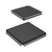
R5S72030W200FP Renesas Electronics America, R5S72030W200FP Datasheet - Page 69

R5S72030W200FP
Manufacturer Part Number
R5S72030W200FP
Description
IC SUPERH MPU ROMLESS 240QFP
Manufacturer
Renesas Electronics America
Series
SuperH® SH7200r
Specifications of R5S72030W200FP
Core Processor
SH2A-FPU
Core Size
32-Bit
Speed
200MHz
Connectivity
CAN, I²C, SCI, SSI, SSU, USB
Peripherals
DMA, LCD, POR, PWM, WDT
Number Of I /o
82
Program Memory Type
ROMless
Ram Size
80K x 8
Voltage - Supply (vcc/vdd)
1.1 V ~ 3.6 V
Data Converters
A/D 8x10b; D/A 2x8b
Oscillator Type
Internal
Operating Temperature
-20°C ~ 85°C
Package / Case
240-QFP
For Use With
R0K572030S000BE - KIT DEV FOR SH7203HS0005KCU11H - EMULATOR E10A-USB H8S(X),SH2(A)
Lead Free Status / RoHS Status
Contains lead / RoHS non-compliant
Eeprom Size
-
Program Memory Size
-
Available stocks
Company
Part Number
Manufacturer
Quantity
Price
Company:
Part Number:
R5S72030W200FP
Manufacturer:
SAMSUNG
Quantity:
1 001
Company:
Part Number:
R5S72030W200FP
Manufacturer:
Renesas Electronics America
Quantity:
10 000
- Current page: 69 of 503
- Download datasheet (3Mb)
Table 5.2 shows the format used in tables 5.3 to 5.8, which list instruction codes, operation, and
execution states in order by classification.
Table 5.2
Notes: 1. Depending on the operand size, displacement is scaled ×1, ×2, or ×4. For details, see
Item
Instruction
Instruction code
Operation
Execution cycles
T bit
2. Instruction execution cycles: The execution cycles shown in the table are minimums.
section 5, Instruction Descriptions.
The actual number of cycles may be increased when (1) contention occurs between
instruction fetches and data access, or (2) when the destination register of the load
instruction (memory → register) and the register used by the next instruction are the
same.
Instruction Code Format
Format
MSB ↔ LSB
→, ←
(xx)
M/Q/T
&
|
^
~
<<n
>>n
—
—
Explanation
Rm:
Rn:
imm:
disp:
mmmm: Source register
nnnn:
iiii:
dddd:
Direction of transfer
Memory operand
Flag bits in the SR
Logical AND of each bit
Logical OR of each bit
Exclusive OR of each bit
Logical NOT of each bit
n-bit left shift
n-bit right shift
Value when no wait states are inserted *
Value of T bit after instruction is executed.
An em-dash (—) in the column means no change.
Source register
Destination register
Immediate data
Displacement *
Destination register
0000: R0
0001: R1
1111: R15
Immediate data
Displacement
⋅
⋅
⋅
Rev. 3.00 Jul 08, 2005 page 53 of 484
1
Section 5 Instruction Set
REJ09B0051-0300
2
Related parts for R5S72030W200FP
Image
Part Number
Description
Manufacturer
Datasheet
Request
R

Part Number:
Description:
KIT STARTER FOR M16C/29
Manufacturer:
Renesas Electronics America
Datasheet:

Part Number:
Description:
KIT STARTER FOR R8C/2D
Manufacturer:
Renesas Electronics America
Datasheet:

Part Number:
Description:
R0K33062P STARTER KIT
Manufacturer:
Renesas Electronics America
Datasheet:

Part Number:
Description:
KIT STARTER FOR R8C/23 E8A
Manufacturer:
Renesas Electronics America
Datasheet:

Part Number:
Description:
KIT STARTER FOR R8C/25
Manufacturer:
Renesas Electronics America
Datasheet:

Part Number:
Description:
KIT STARTER H8S2456 SHARPE DSPLY
Manufacturer:
Renesas Electronics America
Datasheet:

Part Number:
Description:
KIT STARTER FOR R8C38C
Manufacturer:
Renesas Electronics America
Datasheet:

Part Number:
Description:
KIT STARTER FOR R8C35C
Manufacturer:
Renesas Electronics America
Datasheet:

Part Number:
Description:
KIT STARTER FOR R8CL3AC+LCD APPS
Manufacturer:
Renesas Electronics America
Datasheet:

Part Number:
Description:
KIT STARTER FOR RX610
Manufacturer:
Renesas Electronics America
Datasheet:

Part Number:
Description:
KIT STARTER FOR R32C/118
Manufacturer:
Renesas Electronics America
Datasheet:

Part Number:
Description:
KIT DEV RSK-R8C/26-29
Manufacturer:
Renesas Electronics America
Datasheet:

Part Number:
Description:
KIT STARTER FOR SH7124
Manufacturer:
Renesas Electronics America
Datasheet:

Part Number:
Description:
KIT STARTER FOR H8SX/1622
Manufacturer:
Renesas Electronics America
Datasheet:

Part Number:
Description:
KIT DEV FOR SH7203
Manufacturer:
Renesas Electronics America
Datasheet:


