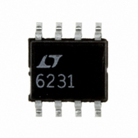
LT6231CS8#PBF Linear Technology, LT6231CS8#PBF Datasheet - Page 9

LT6231CS8#PBF
Manufacturer Part Number
LT6231CS8#PBF
Description
IC OP AMP DUAL LP 3.4MA 8-SOIC
Manufacturer
Linear Technology
Datasheet
1.LT6230CS6TRMPBF.pdf
(24 pages)
Specifications of LT6231CS8#PBF
Amplifier Type
General Purpose
Number Of Circuits
2
Output Type
Rail-to-Rail
Slew Rate
70 V/µs
Gain Bandwidth Product
215MHz
Current - Input Bias
5µA
Voltage - Input Offset
50µV
Current - Supply
3.3mA
Current - Output / Channel
30mA
Voltage - Supply, Single/dual (±)
3 V ~ 12.6 V, ±1.5 V ~ 6.3 V
Operating Temperature
-40°C ~ 85°C
Mounting Type
Surface Mount
Package / Case
8-SOIC (3.9mm Width)
Lead Free Status / RoHS Status
Lead free / RoHS Compliant
-3db Bandwidth
-
Available stocks
Company
Part Number
Manufacturer
Quantity
Price
elecTrical characTerisTics
temperature range. V
SYMBOL
V
V
I
I
A
V
CMRR
PSRR
V
V
I
I
I
V
V
t
t
SR
FPBW
Note 1: Stresses beyond those listed under Absolute Maximum Ratings
may cause permanent damage to the device. Exposure to any Absolute
Maximum Rating condition for extended periods may affect device
reliability and lifetime.
Note 2: Inputs are protected by back-to-back diodes. If the differential
input voltage exceeds 0.7V, the input current must be limited to less than
40mA.
Note 3: A heat sink may be required to keep the junction temperature
below the absolute maximum rating when the output is shorted
indefinitely.
B
OS
SC
S
ENABLE
ON
OFF
OS
OS
VOL
CM
OL
OH
L
H
TC
PARAMETER
Input Offset Voltage
Input Offset Voltage Match
(Channel-to-Channel) (Note 6)
Input Offset Voltage Drift (Note 10)
Input Bias Current
I
Input Offset Current
Large-Signal Gain
Input Voltage Range
Common Mode Rejection Ratio
CMRR Match (Channel-to-Channel) (Note 6) V
Power Supply Rejection Ratio
PSRR Match (Channel-to-Channel) (Note 6)
Output Voltage Swing Low (Note 8)
Output Voltage Swing High (Note 8)
Short-Circuit Current
Supply Current per Amplifier
Disabled Supply Current per Amplifier
ENABLE Pin Current
ENABLE Pin Input Voltage Low
ENABLE Pin Input Voltage High
Output Leakage Current
Turn-On Time
Turn-Off Time
Slew Rate
Full-Power Bandwidth (Note 9)
B
Match (Channel-to-Channel) (Note 6)
S
= ±5V, V
CM
= V
OUT
= 0V, ENABLE = 0V, unless otherwise noted. (Note 5)
CONDITIONS
LT6230I, LT6230I-10
LT6231IS8, LT6232IGN
LT6231IDD
V
V
V
Guaranteed by CMRR
V
V
V
No Load
I
I
No Load
I
I
ENABLE = 4.8V
ENABLE = 0.3V
ENABLE = 4.8V, V
ENABLE = 5V to 0V, R
ENABLE = 0V to 5V, R
A
LT6230-10, A
V
SINK
SINK
SOURCE
SOURCE
O
O
O
CM
CM
S
S
V
OUT
= ±1.5V to ±5V
= ±1.5V to ±5V
= –1, R
= ±4.5V, R
= ±4.5V, R
= ±1.5V, R
= –3V to 4V
= –3V to 4V
= 5mA
= 15mA
= 3V
The
= 5mA
= 20mA
P-P
L
= 1k, V
l
; LT6230I, LT6231I, LT6232I
L
L
L
V
denotes the specifications which apply over the –40°C < T
= 10k
= 1k
= 100Ω
= –10, R
O
O
= ±1V
Note 4: The LT6230C/LT6230I the LT6231C/LT6231I, and LT6232C/LT6232I
are guaranteed functional over the temperature range of –40°C and 85°C.
Note 5: The LT6230C/LT6231C/LT6232C are guaranteed to meet specified
performance from 0°C to 70°C. The LT6230C/LT6231C/LT6232C are
designed, characterized and expected to meet specified performance from
–40°C to 85°C, but are not tested or QA sampled at these temperatures.
The LT6230I/LT6231I/LT6232I are guaranteed to meet specified
performance from –40°C to 85°C.
= –2V to 2V
L
L
= 1k
= 1k
L
= 1k, V
O
= –2V to 2V
LT6230/LT6230-10
l
l
l
l
l
l
l
l
l
l
l
l
l
l
l
l
l
l
l
l
l
l
l
l
l
l
l
l
l
l
l
l
l
l
MIN
±15
LT6231/LT6232
4.8
4.8
3.9
93
25
–3
95
89
85
79
37
TYP
300
260
0.5
72
1
1
1000
–110
MAX
4.85
700
550
650
210
510
220
675
1.1
0.8
0.3
12
60
70
3
4
A
< 85°C
623012fc
UNITS
µV/°C
V/mV
V/mV
V/mV
9
V/µs
V/µs
MHz
mV
mV
mV
mV
mV
mV
mA
mA
µV
µV
µV
µV
µA
µA
µA
dB
dB
dB
dB
µA
µA
µA
ns
µs
V
V
V


