LPV324M/NOPB National Semiconductor, LPV324M/NOPB Datasheet
LPV324M/NOPB
Specifications of LPV324M/NOPB
*LPV324M/NOPB
LPV324M


Related parts for LPV324M/NOPB

LPV324M/NOPB Summary of contents
Page 1
... BiCMOS process. The LPV321/358/324 have bipolar input and output stages for improved noise perfor- mance and higher output current drive. Connection Diagrams 5-Pin SC70/SOT23 10092001 Top View © 2006 National Semiconductor Corporation Features + (For and V j Guaranteed 2.7V and 5V performance j ...
Page 2
... Absolute Maximum Ratings If Military/Aerospace specified devices are required, please contact the National Semiconductor Sales Office/ Distributors for availability and specifications. ESD Tolerance (Note 2) Human Body Model LPV324 LPV358 LPV321 Machine Model Differential Input Voltage + − Supply Voltage (V – Output Short Circuit to V − ...
Page 3
DC Electrical Characteristics Unless otherwise specified, all limits guaranteed for T Boldface limits apply at the temperature extremes. Symbol Parameter V Input Offset Voltage OS TCV Input Offset Voltage Average OS Drift I Input Bias Current B I Input ...
Page 4
AC Electrical Characteristics Note 1: Absolute Maximum Ratings indicate limits beyond which damage to the device may occur. Operating Ratings indicate conditions for which the device is intended to be functional, but specific performance is not guaranteed. For guaranteed ...
Page 5
Typical Performance Characteristics T = 25˚C. A Supply Current vs. Supply Voltage (LPV321) Sourcing Current vs. Output Voltage Sinking Current vs. Output Voltage Unless otherwise specified, V Input Current vs. Temperature 100920B4 Sourcing Current vs. Output Voltage 10092041 Sinking Current ...
Page 6
Typical Performance Characteristics T = 25˚C. (Continued) A Output Voltage Swing vs. Supply Voltage Input Current Noise vs Frequency Crosstalk Rejection vs. Frequency www.national.com Unless otherwise specified, V Input Voltage Noise vs. 100920B6 Input Current Noise vs Frequency 10092070 PSRR ...
Page 7
Typical Performance Characteristics T = 25˚C. (Continued) A CMRR vs. Frequency CMRR vs. Input Common Mode Voltage ∆V vs Unless otherwise specified, V CMRR vs. Input Common Mode Voltage 10092063 10092065 Input Voltage vs. Output Voltage 10092046 ...
Page 8
Typical Performance Characteristics T = 25˚C. (Continued) A Input Voltage vs. Output Voltage Open Loop Frequency Response Gain and Phase vs. Capacitive Load www.national.com Unless otherwise specified, V Open Loop Frequency Response 10092071 Gain and Phase vs. Capacitive Load 10092051 ...
Page 9
Typical Performance Characteristics T = 25˚C. (Continued) A Non-Inverting Large Signal Pulse Response Inverting Large Signal Pulse Response Stability vs. Capacitive Load Unless otherwise specified, V Non-Inverting Small Signal Pulse Response 10092050 Inverting Small Signal Pulse Response 10092047 Stability vs. ...
Page 10
Typical Performance Characteristics T = 25˚C. (Continued) A Stability vs. Capacitive Load THD vs. Frequency Short Circuit Current vs. Temperature (Sinking) www.national.com Unless otherwise specified, V Stability vs. Capacitive Load 10092059 Open Loop Output Impedance vs Frequency 10092062 Short Circuit ...
Page 11
Application Information BENEFITS OF THE LPV321/358/324 Size The small footprints of the LPV321/358/324 packages save space on printed circuit boards, and enable the design of smaller electronic products, such as cellular phones, pagers, or other portable systems. The low profile ...
Page 12
Application Information FIGURE 3. Indirectly Driving A Capacitive Load with DC Accuracy INPUT BIAS CURRENT CANCELLATION The LPV321/358/324 family has a bipolar input stage. The typical input bias current of LPV321/358/324 is 1.5 nA with 5V supply. Thus a 100 ...
Page 13
Application Information Two-op-amp Instrumentation Amplifier A two-op-amp instrumentation amplifier can also be used to make a high-input-impedance DC differential amplifier (Fig- ure 7 the three-op-amp circuit, this instrumentation amplifier requires precise resistor matching for good CMRR. R should ...
Page 14
SC70-5 Tape and Reel Specification SOT-23-5 Tape and Reel Specification TAPE FORMAT Tape Section Leader (Start End) Carrier Trailer (Hub End) www.national.com # Cavities Cavity Status 0 (min) Empty 75 (min) Empty 3000 Filled 250 Filled 125 (min) Empty 0 ...
Page 15
SOT-23-5 Tape and Reel Specification TAPE DIMENSIONS 8 mm 0.130 0.124 (3.3) (3.15) Tape Size DIM A DIM Ao (Continued) ± 0.130 0.126 0.138 0.002 ± (3.3) (3.2) (3.5 0.05) DIM B DIM Bo DIM F 15 100920B1 ± ± ...
Page 16
SOT-23-5 Tape and Reel Specification REEL DIMENSIONS 8 mm 7.00 0.059 0.512 0.795 2.165 330.00 1.50 Tape Size A www.national.com (Continued) 0.331 + 0.059/−0.000 13.00 20.20 55.00 8.40 + 1.50/−0. 100920B2 0.567 W1+ 0.078/−0.039 ...
Page 17
Physical Dimensions inches (millimeters) unless otherwise noted Physical Dimensions 5-Pin SC70 NS Package Number MAA05A 5-Pin SOT23 NS Package Number MF05A 17 www.national.com ...
Page 18
Physical Dimensions www.national.com inches (millimeters) unless otherwise noted (Continued) 8-Pin SOIC NS Package Number M08A 8-Pin MSOP NS Package Number MUA08A 18 ...
Page 19
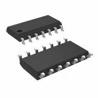
Physical Dimensions inches (millimeters) unless otherwise noted (Continued) 14-Pin SOIC NS Package Number M14A 14-Pin TSSOP NS Package Number MTC14 19 www.national.com ...
Page 20
... BANNED SUBSTANCE COMPLIANCE National Semiconductor follows the provisions of the Product Stewardship Guide for Customers (CSP-9-111C2) and Banned Substances and Materials of Interest Specification (CSP-9-111S2) for regulatory environmental compliance. Details may be found at: www.national.com/quality/green. ...