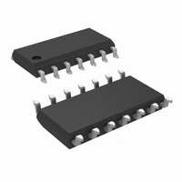
LMH6644MA/NOPB National Semiconductor, LMH6644MA/NOPB Datasheet - Page 16

LMH6644MA/NOPB
Manufacturer Part Number
LMH6644MA/NOPB
Description
IC AMP R-R I/O 3V 130MHZ 14-SOIC
Manufacturer
National Semiconductor
Series
PowerWise®r
Type
Voltage Feedback Amplifierr
Datasheet
1.LMH6642MFNOPB.pdf
(22 pages)
Specifications of LMH6644MA/NOPB
Amplifier Type
Voltage Feedback
Number Of Circuits
4
Output Type
Rail-to-Rail
Slew Rate
135 V/µs
-3db Bandwidth
130MHz
Current - Input Bias
20nA
Voltage - Input Offset
1000µV
Current - Supply
2.7mA
Current - Output / Channel
75mA
Voltage - Supply, Single/dual (±)
2.7 V ~ 12.8 V, ±1.35 V ~ 6.4 V
Operating Temperature
-40°C ~ 85°C
Mounting Type
Surface Mount
Package / Case
14-SOIC (3.9mm Width), 14-SOL
Rail/rail I/o Type
Rail to Rail Output
Number Of Elements
4
Common Mode Rejection Ratio
72dB
Input Offset Voltage
5mV
Input Bias Current
2.6uA
Single Supply Voltage (typ)
3/5/9/12V
Dual Supply Voltage (typ)
±3/±5V
Voltage Gain In Db
98dB
Power Supply Rejection Ratio
79dB
Power Supply Requirement
Single/Dual
Shut Down Feature
No
Single Supply Voltage (min)
2.7V
Single Supply Voltage (max)
12.8V
Dual Supply Voltage (min)
±1.35V
Dual Supply Voltage (max)
±6.4V
Technology
BiCOM
Operating Temp Range
-40C to 85C
Operating Temperature Classification
Industrial
Mounting
Surface Mount
Pin Count
14
Package Type
SOIC N
Number Of Channels
4
Voltage Gain Db
98 dB
Common Mode Rejection Ratio (min)
72 dB
Input Voltage Range (max)
12.8 V
Input Voltage Range (min)
2.7 V
Operating Supply Voltage
3 V, 5 V, 9 V, 12 V
Supply Current
17 mA at 5 V
Maximum Operating Temperature
+ 85 C
Mounting Style
SMD/SMT
Maximum Dual Supply Voltage
+/- 6.4 V
Minimum Operating Temperature
- 40 C
Lead Free Status / RoHS Status
Lead free / RoHS Compliant
Gain Bandwidth Product
-
Lead Free Status / Rohs Status
Compliant
Other names
*LMH6644MA
*LMH6644MA/NOPB
LMH6644MA
*LMH6644MA/NOPB
LMH6644MA
www.national.com
Application Information
CIRCUIT DESCRIPTION
The LMH664X family is based on National Semiconductor’s
proprietary VIP10 dielectrically isolated bipolar process.
This device family architecture features the following:
•
•
•
•
•
Application Hints
This Op Amp family is a drop-in replacement for the AD805X
family of high speed Op Amps in most applications. In addi-
tion, the LMH664X will typically save about 40% on power
dissipation, due to lower supply current, when compared to
competition. All AD805X family’s guaranteed parameters are
included in the list of LMH664X guaranteed specifications in
order to ensure equal or better level of performance. Howev-
er, as in most high performance parts, due to subtleties of
applications, it is strongly recommended that the performance
of the part to be evaluated is tested under actual operating
conditions to ensure full compliance to all specifications.
With 3V supplies and a common mode input voltage range
that extends 0.5V below V
in low voltage/low power applications. Even with 3V supplies,
the −3dB BW (@ A
limit of 80MHz. Production testing guarantees that process
variations with not compromise speed. High frequency re-
sponse is exceptionally stable confining the typical −3dB BW
over the industrial temperature range to ±2.5%.
As can be seen from the typical performance plots, the
LMH664X output current capability (
compared to AD805X. This enhancement, increases the out-
put load range, adding to the LMH664X’s versatility.
Because of the LMH664X’s high output current capability at-
tention should be given to device junction temperature in
order not to exceed the Absolute Maximum Rating.
Complimentary bipolar devices with exceptionally high f
(
bias current.
A class A-B “turn-around” stage with improved noise,
offset, and reduced power dissipation compared to similar
speed devices (patent pending).
Common Emitter push-push output stage capable of
75mA output current (at 0.5V from the supply rails) while
consuming only 2.7mA of total supply current per channel.
This architecture allows output to reach within milli-volts of
either supply rail.
Consistent performance over the entire operating supply
voltage range with little variation for the most important
specifications (e.g. BW, SR, I
Significant power saving (
devices on the market with similar performance.
∼
8GHz) even under low supply voltage (2.7V) and low
V
= +1) is typically 115MHz with a tested
−
, the LMH664X find applications
∼
40%) compared to competitive
OUT
, etc.)
∼
75mA) is enhanced
t
16
This device family was designed to avoid output phase re-
versal. With input overdrive, the output is kept near supply rail
(or as closed to it as mandated by the closed loop gain setting
and the input voltage). See
FIGURE 1. Input and Output Shown with CMVR Exceeded
However, if the input voltage range of −0.5V to 1V from V
exceeded by more than a diode drop, the internal ESD pro-
tection diodes will start to conduct. The current in the diodes
should be kept at or below 10mA.
Output overdrive recovery time is less than 100ns as can be
seen from
FIGURE 2. Overload Recovery Waveform
Figure 2
plot:
Figure
1:
20018543
20018542
+
is


