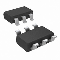
LPV531MK/NOPB National Semiconductor, LPV531MK/NOPB Datasheet - Page 13

LPV531MK/NOPB
Manufacturer Part Number
LPV531MK/NOPB
Description
IC OPAMP PROG R-R OUT TSOT23-6
Manufacturer
National Semiconductor
Series
PowerWise®r
Datasheet
1.LPV531MKNOPB.pdf
(17 pages)
Specifications of LPV531MK/NOPB
Amplifier Type
General Purpose
Number Of Circuits
1
Output Type
Rail-to-Rail
Slew Rate
2.5 V/µs
Gain Bandwidth Product
4.6MHz
Current - Input Bias
0.05pA
Voltage - Input Offset
1000µV
Current - Supply
425µA
Current - Output / Channel
24mA
Voltage - Supply, Single/dual (±)
2.7 V ~ 5.5 V
Operating Temperature
-40°C ~ 85°C
Mounting Type
Surface Mount
Package / Case
TSOT-23-6, TSOT-6
Number Of Channels
1
Voltage Gain Db
128 dB
Common Mode Rejection Ratio (min)
72 dB
Input Offset Voltage
4.5 mV at 5 V
Operating Supply Voltage
5 V
Supply Current
0.53 mA at 5 V
Maximum Operating Temperature
+ 85 C
Minimum Operating Temperature
- 40 C
Lead Free Status / RoHS Status
Lead free / RoHS Compliant
-3db Bandwidth
-
Lead Free Status / Rohs Status
Details
Other names
LPV531MK
LPV531MKTR
LPV531MKTR
Application Information
2. Switched Discrete Power Modes
In this typical application, the LPV531 can operate at two (or
more) power modes in order to fulfill the demands of the
design. One of the modes is used to save power. It is a low
power mode which is set by using a large resistor. The
others are the higher power modes which are set by one or
more smaller resistors. The larger resistor that sets the low
power mode can be permanently connected while the
smaller resistor(s) can be switched in parallel to set the high
power mode(s). This configuration allows the designer to get
the required performance from the LPV531 when needed.
The switches shown in Figure 3 can be easily implemented
with an open drain I/O port of an ASIC or any other simple
pull down switch.
3. DAC Controlled Power Modes
For voltage controlled filter applications, where control of the
gain bandwidth is essential, a DAC and a resistive voltage
divider can be used. In this application the current drawn
from the I
output range is divided to match the V
has the range of 0-110 mV.
FIGURE 4. DAC Controlled Power Mode Configurations
FIGURE 3. Power Modes Set by Resistors and
SEL
pin is controlled by the DAC. The DAC’s total
Switches
−
to V
(Continued)
INT
voltage which
20132364
20132363
13
The output of the resistive voltage divider should have an
impedance that is small compared to the value of R
allow a linear control of the power level. Therefore, R
needs to have a value in the order of R
R
mode operation, these resistor values will divide the maxi-
mum voltage of V
DETERMINING THE R
To determine the value of R
supply current or bandwidth, the following equations can be
used:
For the power modes characterized in this datasheet, these
formulas lead to the values in Table 1. These values deviate
slightly from the typical values presented in the electrical
characteristic tables. The values in Table 1 are calculated
using approximated linear equations while the values in the
Electrical Characteristics table are the result of characteriza-
tion measurement procedures.
To calculate the R
a minimum output current at all times and over all tempera-
tures, use the following equations:
If the output has to be kept at V
tance, the required R
equations:
EXT1
100 kΩ
1 MΩ
R
1Ω
EXT
= 125 mV * R
TABLE 1. Values for Characterized
0.9 µA
99 nA
9 µA
I
SEL
CONTROL
EXT
EXT
EXT2
which will allow the LPV531 to deliver
Power Modes
Supply Current
EXT
can be calculated with the following
/V
400 µA
to 125 mV.
5.3 µA
VALUES AND I
40 µA
EXT
or
CONTROL,MAX
that is needed for a certain
+
/2 for a known load resis-
. For 1 µA power
Gain Bandwidth
SEL
Product
4.6 MHz
460 kHz
60 kHz
LEVELS
INT
www.national.com
/10 and
INT
EXT2
to


