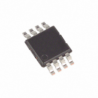
MAX4208AUA+ Maxim Integrated Products, MAX4208AUA+ Datasheet - Page 6

MAX4208AUA+
Manufacturer Part Number
MAX4208AUA+
Description
IC INSTRUMENT AMP PREC 8-UMAX
Manufacturer
Maxim Integrated Products
Datasheet
1.MAX4209EVKIT.pdf
(17 pages)
Specifications of MAX4208AUA+
Amplifier Type
Instrumentation
Number Of Circuits
1
Output Type
Rail-to-Rail
Slew Rate
0.08 V/µs
Gain Bandwidth Product
750kHz
Current - Input Bias
1pA
Voltage - Input Offset
3µV
Current - Supply
1.4mA
Current - Output / Channel
25mA
Voltage - Supply, Single/dual (±)
2.85 V ~ 5.5 V, ±1.425 V ~ 2.25 V
Operating Temperature
-40°C ~ 125°C
Mounting Type
Surface Mount
Package / Case
8-MSOP, Micro8™, 8-uMAX, 8-uSOP,
Number Of Channels
Single
Common Mode Rejection Ratio (min)
106 dB
Input Offset Voltage
0.02 mV
Input Bias Current (max)
0.000001 uA
Operating Supply Voltage
3 V, 5 V
Supply Current
2.3 mA
Maximum Power Dissipation
362 mW
Maximum Operating Temperature
+ 125 C
Minimum Operating Temperature
- 40 C
Mounting Style
SMD/SMT
Maximum Dual Supply Voltage
+/- 2.75 V
Minimum Dual Supply Voltage
+/- 1.425 V
Supply Voltage (max)
5.5 V
Supply Voltage (min)
2.85 V
No. Of Amplifiers
1
Bandwidth
750kHz
Amplifier Output
Rail To Rail
Cmrr
135dB
Supply Voltage Range
± 1.425V To ± 2.75V
Rohs Compliant
Yes
Lead Free Status / RoHS Status
Lead free / RoHS Compliant
-3db Bandwidth
-
Lead Free Status / Rohs Status
Lead free / RoHS Compliant
Ultra-Low Offset/Drift, Precision
Instrumentation Amplifiers with REF Buffer
ELECTRICAL CHARACTERISTICS (continued)
(V
G = 100V/V (R1 = 1kΩ, R2 = 99kΩ), T
Note 1: Specifications are 100% production tested at +25°C, unless otherwise noted. Limits over temperature are guaranteed by design.
Note 2: Guaranteed by design. Thermocouple and leakage effects preclude measurement of this parameter during production testing.
Note 3: IN+ and IN- are gates to CMOS transistors with typical input bias current of 1pA. CMOS leakage is so small that it is impractical to
Note 4: Setting REF to ground (V
Note 5: This is the REF current needed to directly drive the end terminal of the gain-setting resistors when REFIN/MODE is connected to
Note 6: Output swing high (V
Note 7: Maximum range for V
Note 8: At G = 100V/V and G = 1000V/V, these instrumentation amplifiers are bandwidth limited and not capable of slew-rate-limited dV/dt.
6
REFIN/MODE Input-Voltage
High
REFIN/MODE Buffer
Common-Mode Rejection Ratio
REF Common-Mode Range
(Note 4)
REF Common-Mode Rejection
Ratio
REFIN/MODE Buffer
Power-Supply Rejection Ratio
OUTPUT DC CHARACTERISTICS
Output-Voltage Swing (Note 6)
POWER SUPPLY
Supply Voltage
Supply Current
DD
_______________________________________________________________________________________
= 5V, V
Devices are screened during production testing to eliminate defective units.
test and guarantee in production. Max V
units. For the MAX4208, when there are no external resistors, the input bias current at FB and REF is 1pA (typ).
and (V
REFIN/MODE to V
V
±100µA and 3.4µA, respectively at +25°C. See the Detailed Description.
and G = 10 have output swing high limited by the range of V
PARAMETER
SS
to put the buffer in high-impedance mode. The REF input current is tested at the gain of 100. At gain 10 and 1000, I
SS
DD
= 0V, V
- 1.3V). In this range, V
CM
DD
= V
OH
puts the part in shutdown (I
DIFF
REF
) and output swing low (V
SS
is from -100mV to +100mV.
) is allowed if the REF buffer is off. The unity-gain buffer is on when V
= V
A
SYMBOL
= -40°C to +125°C, unless otherwise noted.) (Note 1)
V
DD
V
V
V
OH
DD
OL
IH
REF
/2, V
= V
REFIN/MODE
DIFF
REFIN/MODE
MAX4208/MAX4209 in shutdown
(V
≤ V
(V
Guaranteed by REF CMRR test
V
1.6V)
V
V
= (V
V
V
Guaranteed by PSRR test
V
buffer OFF
(V
(V
REFIN/MODE = V
SS
D D
REFIN/MODE
DD
OUT
REFIN/MODE
SS
DD
SS
DD
is ±100mV. Devices are screened during production testing to eliminate defective
REF
SS
≤ V
= 2.85V to 5.5V ,
- V
+ 0.2V)
+ 0.2V) ≤ V
- 1.6V)
- 1.6V), buffer ON
- V
OL
+ 0.5V)
≤
OUT
DD
REF
SS
) are measured only on G = 100 and G = 1000 devices. Devices with G = 1
= V
= 1.4µA).
±40µV (maximum buffer input offset voltage over temperature). Setting
≤ (V
SS
= V
= V
, R
CONDITIONS
DD
REFIN/MODE
REF
SS
CM
DD
L
-
,
= 100kΩ to V
, V
, shutdown mode
T
T
A
A
T
T
T
T
R
R
R
R
R
R
CM
A
A
A
A
= +25°C to +85°C
= -40°C to +125°C
L
L
L
L
L
L
= +25°C to +85°C
= - 40°C to + 125°C
= +25°C to +85°C
= - 40°C to + 125°C
= 100kΩ
= 10kΩ
= 1kΩ
= 100kΩ
= 10kΩ
= 1kΩ
, and V
≤
V
V
DIFF
DD
DD
DD
/2, V
(see the Output Swing section).
= 5V
= 5V
DIFF
= (V
V
MIN
2.85
V
DD
0.2
96
90
96
96
90
90
SS
IN+
-
- V
REFIN/MODE
IN-
TYP
) = 0V, MAX4208 set for
V
MAX
is between 0.15V
5.50
1.70
375
325
1.6
3.0
DD
60
90
50
75
10
-
REF
UNITS
mV
mA
dB
dB
dB
µA
=
V
V
V


