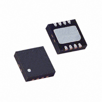
LT6231CDD#TR Linear Technology, LT6231CDD#TR Datasheet

LT6231CDD#TR
Specifications of LT6231CDD#TR
Available stocks
Related parts for LT6231CDD#TR
LT6231CDD#TR Summary of contents
Page 1
... The LT6232 is available in the 16-pin SSOP package. L, LT, LTC, LTM, Linear Technology and the Linear logo are registered trademarks of Linear Technology Corporation. ThinSOT is a trademark of Linear Technology Corporation. All other trademarks are the property of their respective owners. ...
Page 2
LT6230/LT6230-10 LT6231/LT6232 absoluTe MaxiMuM raTings + – Total Supply Voltage ( .............................. 12.6V Input Current (Note 2) ......................................... ±40mA Output Short-Circuit Duration (Note 3) ............ Indefinite Operating Temperature Range (Note 4)....–40°C to 85°C Specified Temperature Range (Note ...
Page 3
... LT6230CS6-10#TRPBF LT6230IS6-10#PBF LT6230IS6-10#TRPBF LT6231CS8#PBF LT6230CS8#TRPBF LT6231IS8#PBF LT6230IS8#TRPBF LT6231CDD#PBF LT6231CDD#TRPBF LT6231IDD#PBF LT6231IDD#TRPBF LT6232CGN#PBF LT6232CGN#TRPBF LT6232IGN#PBF LT6232IGN#TRPBF Consult LTC Marketing for parts specified with wider operating temperature ranges. *The temperature grade is identified by a label on the shipping container. Consult LTC Marketing for information on non-standard lead based finish parts. ...
Page 4
LT6230/LT6230-10 LT6231/LT6232 elecTrical characTerisTics ENABLE = 0V, unless otherwise noted. SYMBOL PARAMETER PSRR Power Supply Rejection Ratio PSRR Match (Channel-to-Channel) (Note 6) Minimum Supply Voltage (Note 7) V Output Voltage Swing Low (Note Output Voltage Swing High ...
Page 5
V = 5V, 0V 3.3V, 0V SYMBOL PARAMETER V Input Offset Voltage OS Input Offset Voltage Match (Channel-to-Channel) (Note Input Offset Voltage Drift (Note 10 Input ...
Page 6
LT6230/LT6230-10 LT6231/LT6232 elecTrical characTerisTics temperature range 5V, 0V 3.3V, 0V SYMBOL PARAMETER V Input Offset Voltage OS Input Offset Voltage Match (Channel-to-Channel) (Note Input Offset Voltage Drift (Note 10) OS ...
Page 7
SYMBOL PARAMETER V Input Offset Voltage OS Input Offset Voltage Match (Channel-to-Channel) (Note 6) I Input Bias Current B I Match (Channel-to-Channel) (Note Input Offset Current OS Input Noise Voltage e Input Noise Voltage Density ...
Page 8
LT6230/LT6230-10 LT6231/LT6232 elecTrical characTerisTics temperature range ±5V OUT SYMBOL PARAMETER V Input Offset Voltage OS Input Offset Voltage Match (Channel-to-Channel) (Note Input Offset Voltage Drift (Note 10 Input ...
Page 9
V = ±5V OUT SYMBOL PARAMETER V Input Offset Voltage OS Input Offset Voltage Match (Channel-to-Channel) (Note Input Offset Voltage Drift (Note 10 Input Bias Current ...
Page 10
LT6230/LT6230-10 LT6231/LT6232 elecTrical characTerisTics Note 6: Matching parameters are the difference between the two amplifiers A and D and between B and C of the LT6232; between the two amplifiers of the LT6231. CMRR and PSRR match are defined as ...
Page 11
Typical perForMance characTerisTics (LT6230/LT6231/LT6232) Output Saturation Voltage vs Load Current (Output High 5V 125° –55° 25°C A 0.01 0.001 0.01 0 LOAD CURRENT ...
Page 12
LT6230/LT6230-10 LT6231/LT6232 Typical perForMance characTerisTics (LT6230/LT6231/LT6232) Noise Voltage and Unbalanced Noise Current vs Frequency ±2. 25° NOISE CURRENT ...
Page 13
Typical perForMance characTerisTics (LT6230/LT6231/LT6232) Power Supply Rejection Ratio vs Frequency 120 25° 100 POSITIVE SUPPLY 60 NEGATIVE SUPPLY 10k 100k 1M ...
Page 14
LT6230/LT6230-10 LT6231/LT6232 Typical perForMance characTerisTics (LT6230/LT6231/LT6232) Distortion vs Frequency – ± 100 , 3RD V L – P-P OUT – 100 , 2ND 1k, ...
Page 15
Typical perForMance characTerisTics (LT6230-10) Gain Bandwidth and Phase Margin vs Temperature 1700 ±5V 1500 S GAIN BANDWIDTH 1300 1100 900 PHASE MARGIN V = ± 3V, ...
Page 16
LT6230/LT6230-10 LT6231/LT6232 Typical perForMance characTerisTics (LT6230-10) 2nd and 3rd Harmonic Distortion vs Frequency – ± – P-P OUT R = 100 , 2ND L – 100 , 3RD ...
Page 17
Amplifier Characteristics Figure simplified schematic of the LT6230/LT6231/ LT6232, which has a pair of low noise input transistors Q1 and Q2. A simple current mirror, Q3/Q4, converts the differential signal to a single-ended output, and ...
Page 18
LT6230/LT6230-10 LT6231/LT6232 applicaTions inForMaTion With the amplifier connected in a gain of A can invert with very heavy overdrive. To avoid this inver- sion, limit the input overdrive to 0.5V beyond the power supply rails. ESD The LT6230/LT6231/LT6232 have reverse-biased ...
Page 19
Typical applicaTions Single Supply, Low Noise, Low Power, Bandpass Filter with Gain = 47pF 732 + V C1 0.1µ 1000pF 10k 732 – LT6230 + 10k 0.1µF 623012 F03 Low ...
Page 20
LT6230/LT6230-10 LT6231/LT6232 package DescripTion 0.62 0.95 MAX REF 3.85 MAX 2.62 REF RECOMMENDED SOLDER PAD LAYOUT PER IPC CALCULATOR 0.20 BSC DATUM ‘A’ 0.30 – 0.50 REF NOTE: 1. DIMENSIONS ARE IN MILLIMETERS 2. DRAWING NOT TO SCALE 3. DIMENSIONS ...
Page 21
DescripTion 3.5 ±0.05 1.65 ±0.05 2.10 ±0.05 (2 SIDES) 0.25 ± 0.05 RECOMMENDED SOLDER PAD PITCH AND DIMENSIONS APPLY SOLDER MASK TO AREAS THAT ARE NOT SOLDERED PIN 1 TOP MARK (NOTE 6) 0.200 REF DD Package 8-Lead Plastic ...
Page 22
LT6230/LT6230-10 LT6231/LT6232 package DescripTion .050 BSC .245 MIN .030 ±.005 TYP RECOMMENDED SOLDER PAD LAYOUT .010 – .020 (0.254 – 0.508) .008 – .010 (0.203 – 0.254) NOTE: 1. DIMENSIONS IN 2. DRAWING NOT TO SCALE 3. THESE DIMENSIONS DO ...
Page 23
... Updated ENABLE Pin section in Applications Information Information furnished by Linear Technology Corporation is believed to be accurate and reliable. However, no responsibility is assumed for its use. Linear Technology Corporation makes no representa- tion that the interconnection of its circuits as described herein will not infringe on existing patent rights. ...
Page 24
... Rail-to-Rail Input and Output 1.9nV/√Hz, 3mA Max, 100MHz Gain Bandwidth www.linear.com ● which flows into PD = –I • 1.5k. C1 ensures stability and OUT 100MHz measurement bandwidth, with 623012 TA02b 50ns/DIV OS , 3.5nV/√ 0111 REV C • PRINTED IN USA LINEAR TECHNOLOGY CORPORA TION 2003 623012fc ...


