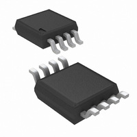
LMH6658MM/NOPB National Semiconductor, LMH6658MM/NOPB Datasheet - Page 16

LMH6658MM/NOPB
Manufacturer Part Number
LMH6658MM/NOPB
Description
IC OPAMP 270MHZ DUAL 8MSOP
Manufacturer
National Semiconductor
Series
PowerWise®r
Datasheet
1.LMH6657MFNOPB.pdf
(20 pages)
Specifications of LMH6658MM/NOPB
Amplifier Type
Voltage Feedback
Number Of Circuits
2
Slew Rate
700 V/µs
Gain Bandwidth Product
140MHz
-3db Bandwidth
270MHz
Current - Input Bias
5µA
Voltage - Input Offset
1000µV
Current - Supply
6.5mA
Current - Output / Channel
110mA
Voltage - Supply, Single/dual (±)
3 V ~ 12 V, ±1.5 V ~ 6 V
Operating Temperature
-40°C ~ 85°C
Mounting Type
Surface Mount
Package / Case
8-MSOP, Micro8™, 8-uMAX, 8-uSOP,
Number Of Channels
2
Voltage Gain Db
95 dB
Common Mode Rejection Ratio (min)
72 dB
Input Offset Voltage
5 mV at 5 V
Operating Supply Voltage
5 V, 9 V
Supply Current
17 mA at 5 V
Maximum Operating Temperature
+ 85 C
Maximum Dual Supply Voltage
+/- 6 V
Minimum Operating Temperature
- 40 C
Lead Free Status / RoHS Status
Lead free / RoHS Compliant
Output Type
-
Lead Free Status / Rohs Status
Details
Other names
LMH6658MM
LMH6658MMTR
LMH6658MMTR
www.national.com
Output Characteristics
OUTPUT CURRENT CAPABILITY
The LMH6657/6658 output swing for a given load can be
determined by referring to the Output Voltage vs. Output
Current plots (Typical Performance Characteristics section).
Characteristic Tables show the output current when the out-
put is 1V from either rail. The plots and table values can be
used to predict closed loop continuous value of current for a
given load. If left unchecked, the output current capability of
the LMH6657/6658 could easily result in junction tempera-
ture exceeding the maximum allowed value specified under
Absolute Maximum Ratings. Proper heat sinking or other
precautions are required if conditions as such, exist.
Under transient conditions, such as when the input voltage
makes a large transition and the output has not had time to
reach its final value, the device can deliver output currents in
excess of the typical plots mentioned above. Plots shown in
Figure 5 and below, depict how the output current capability
improves under higher input overdrive voltages:
The LMH6657/6658 output stage is designed to swing within
approximately one diode drop of each supply voltage by
FIGURE 4. V
FIGURE 5. V
OUT
OUT
vs. I
vs. I
SOURCE
SINK
(for Various Overdrive)
(for Various Overdrive)
20053247
20053248
16
utilizing specially designed high speed output clamps. This
allows adequate output voltage swing even with 5V supplies
and yet avoids some of the issues associated with rail-to-rail
output operational amplifiers. Some of these issues are:
• Supply current increases when output reaches saturation
• Prolonged recovery when output approaches the rails
The LMH6657/6658 output is exceedingly well-behaved
when it comes to recovering from an overload condition. As
can be seen from Figure 6 below, the LMH6657/6658 will
typically recover from an output overload condition in about
18ns, regardless of the duration of the overload.
OUTPUT PHASE REVERSAL
This is a problem with some operational amplifiers. This
effect is caused by phase reversal in the input stage due to
saturation of one or more of the transistors when the inputs
exceed the normal expected range of voltages. Some appli-
cations, such as servo control loops among others, are
sensitive to this kind of behavior and would need special
safeguards to ensure proper functioning. The LMH6657/
6658 is immune to output phase reversal with input overload.
With inputs exceeded, the LMH6657/6658 output will stay at
the clamped voltage from the supply rail. Exceeding the
input supply voltages beyond the Absolute Maximum Rat-
ings of the device could however damage or otherwise ad-
versely effect the reliability or life of the device.
DRIVING CAPACITIVE LOADS
The LMH6657/6658 can drive moderate values of capaci-
tance by utilizing a series isolation resistor between the
output and the capacitive load. Typical Performance Char-
acteristics section shows the settling time behavior for vari-
ous capacitive loads and 20Ω of isolation resistance. Ca-
pacitive load tolerance will improve with higher closed loop
gain values. Applications such as ADC buffers, among oth-
ers, present complex and varying capacitive loads to the Op
Amp; best value for this isolation resistance is often found by
experimentation and actual trial and error for each applica-
tion.
DISTORTION
Applications with demanding distortion performance require-
ments are best served with the device operating in the
inverting mode. The reason for this is that in the inverting
configuration, the input common mode voltage does not vary
at or near the supply rails
FIGURE 6. Output Overload Recovery
20053249


