LP3986BL-2828 National Semiconductor, LP3986BL-2828 Datasheet
LP3986BL-2828
Specifications of LP3986BL-2828
Available stocks


Related parts for LP3986BL-2828


LP3986BL-2828 Summary of contents
Page 1
... The LP3986 is available in a micro SMD package. Perfor- mance is specified for a −40°C to +125°C temperature range. For single LDO applications, please refer to the LP3985 datasheet. Typical Application Circuit © 2007 National Semiconductor Corporation Features ■ Miniature 8-I/O micro SMD package ■ ...
Page 2
Block Diagram Pin Descriptions Name V OUT2 EN BYPASS GND GND EN V OUT1 Note: The pin numbering scheme for the micro SMD package was revised in April 2002 to conform to JEDEC standard. Only the pin ...
Page 3
Ordering Information For micro SMD Package (TL has thickness of 0.600mm) Output Voltage Grade (V) 2.5 2.5 STD 2.5 2.8 STD 2.5 1.8 STD 2.6 2.6 STD 2.8 1.8 STD 2.8 2.8 STD 2.85 2.85 STD 2.9 2.9 STD 3.0 ...
Page 4
... Absolute Maximum Ratings If Military/Aerospace specified devices are required, please contact the National Semiconductor Sales Office/ Distributors for availability and specifications OUT Junction Temperature Storage Temperature Pad Temp. (Note 3) Electrical Characteristics Unless otherwise specified limits appearing in standard typeface are for T range for operation, −40°C to +125°C. (Notes 7, 8) ...
Page 5
... Electrical Characteristics tables. Note 2: All voltages are with respect to the potential at the GND pin. Note 3: Additional information on pad temperature can be found in National Semiconductor Application Note (AN-1112). Note 4: The Absolute Maximum power dissipation depends on the ambient temperature and can be calculated using the formula: is the ambient temperature, and θ ...
Page 6
Test Signals Typical Performance Characteristics 0. 25°C, both enable pins are tied OUT A Power Supply Rejection Ratio (C www.national.com FIGURE 1. Line Regulation Input Test Signal FIGURE 2. PSRR ...
Page 7
Power Supply Rejection Ratio (C BP Line Transient Response (C = 0.001µF) BP Load Transient & Cross Talk ( 0.1µF) Output Noise Spectral Density 20003448 Line Transient Response (C 20003413 + 0.2V) Load Transient & Cross ...
Page 8
Start-Up Time (C = 0.001, 0.01, 0.1µF) BP Enable Response (V IN Output Short Circuit Current at V www.national.com 20003411 = V + 0.2V) OUT 20003415 = 6V Output Short Circuit Current 20003465 8 Enable Response ( ...
Page 9
... MICRO SMD MOUNTING The micro SMD package requires specific mounting tech- ≊ 2.2µF) niques which are detailed in National Semiconductor Appli- cation Note (AN-1112). Referring to the section Surface Mount Technology (SMT) Assembly Considerations. For best results during assembly, alignment ordinals on the PC board may be used to facilitate placement of the micro SMD device ...
Page 10
MICRO SMD LIGHT SENSITIVITY Exposing the micro SMD device to direct sunlight will cause misoperation of the device. Light sources such as halogen lamps can effect electrical performance if brought near to the device. The wavelengths which have most detrimental ...
Page 11
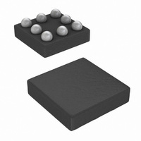
Physical Dimensions inches (millimeters) unless otherwise noted The dimensions for X1, X2 and X3 are as follows: micro SMD, 8 Bump NS Package Number TL08CCA X1 = 1.55mm X2 = 1.55mm X3 = 0.600mm 11 www.national.com ...
Page 12
... National Semiconductor and the National Semiconductor logo are registered trademarks of National Semiconductor Corporation. All other brand or product names may be trademarks or registered trademarks of their respective holders. ...