SI8465DB-T2-E1 Vishay, SI8465DB-T2-E1 Datasheet - Page 7
SI8465DB-T2-E1
Manufacturer Part Number
SI8465DB-T2-E1
Description
MOSFET P-CH D-S 20V MICROFOOT
Manufacturer
Vishay
Series
TrenchFET®r
Datasheet
1.SI8465DB-T2-E1.pdf
(8 pages)
Specifications of SI8465DB-T2-E1
Fet Type
MOSFET P-Channel, Metal Oxide
Fet Feature
Logic Level Gate
Rds On (max) @ Id, Vgs
104 mOhm @ 1.5A, 4.5V
Drain To Source Voltage (vdss)
20V
Vgs(th) (max) @ Id
1.5V @ 250µA
Gate Charge (qg) @ Vgs
18nC @ 10V
Input Capacitance (ciss) @ Vds
450pF @ 10V
Power - Max
780mW
Mounting Type
Surface Mount
Package / Case
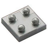
4-MICRO FOOT®CSP
Transistor Polarity
P Channel
Continuous Drain Current Id
-3.8A
Drain Source Voltage Vds
-20V
On Resistance Rds(on)
104mohm
Rds(on) Test Voltage Vgs
-4.5V
Threshold Voltage Vgs Typ
-1.5V
Resistance Drain-source Rds (on)
0.122 Ohms
Forward Transconductance Gfs (max / Min)
7 S
Drain-source Breakdown Voltage
- 20 V
Continuous Drain Current
- 3.8 A
Power Dissipation
1.8 W
Maximum Operating Temperature
+ 85 C
Mounting Style
SMD/SMT
Minimum Operating Temperature
- 40 C
Lead Free Status / RoHS Status
Lead free / RoHS Compliant
Current - Continuous Drain (id) @ 25° C
-
Lead Free Status / Rohs Status
Details
Other names
SI8465DB-T2-E1TR


PACKAGE OUTLINE
MICRO FOOT: 4-BUMP (2 x 2, 0.5 mm PITCH)
Notes (Unless otherwise specified):
1. All dimensions are in millimeters.
2. Four (4) solder bumps are lead (Pb)-free 95.5Sn/3.8Ag/0.7Cu with diameter ∅ 0.30 mm to 0.32 mm.
3. Backside surface is coated with a Ti/Ni/Ag layer.
4. Non-solder mask defined copper landing pad.
5. • is location of pin 1.
Notes:
a. Use millimeters as the primary measurement.
Vishay Siliconix maintains worldwide manufacturing capability. Products may be manufactured at one of several qualified locations. Reliability data for Silicon
Technology and Package Reliability represent a composite of all qualified locations. For related documents such as package/tape drawings, part marking, and
reliability data, see www.vishay.com/ppg?65363.
Document Number: 65363
S09-1922-Rev. A, 28-Sep-09
Dim.
A
A
A
b
D
e
s
1
2
0.462
0.220
0.242
0.300
0.230
0.920
Min.
Mark on Backside of Die
Recommended Land
2
1
8465
X X X
4 x Ø 0.24 to 0.26 Note 4
Solder Mask ~ Ø 0.25
Millimeters
Nom.
0.505
0.250
0.255
0.310
0.500
0.250
0.960
4
3
a
4 x Ø b
0.548
0.280
0.268
0.320
0.270
1.000
Max.
s
S
D
D
e
Bump Note 2
0.0181
0.0086
0.0095
0.0118
0.0090
0.0362
Min.
G
S
Inches
0.0198
0.0098
0.0100
0.0122
0.0197
0.0098
0.0378
Nom.
Vishay Siliconix
Si8465DB
www.vishay.com
0.0215
0.0110
0.0105
0.0126
0.0106
0.0394
Max.
7
Related parts for SI8465DB-T2-E1
Image
Part Number
Description
Manufacturer
Datasheet
Request
R

Part Number:
Description:
P-channel 20-v D-s Mosfet
Manufacturer:
Vishay
Datasheet:
Part Number:
Description:
357-036-542-201 CARDEDGE 36POS DL .156 BLK LOPRO
Manufacturer:
Vishay
Datasheet:
Part Number:
Description:
357-036-542-201 CARDEDGE 36POS DL .156 BLK LOPRO
Manufacturer:
Vishay
Datasheet:
Part Number:
Description:
357-036-542-201 CARDEDGE 36POS DL .156 BLK LOPRO
Manufacturer:
Vishay
Datasheet:
Part Number:
Description:
357-036-542-201 CARDEDGE 36POS DL .156 BLK LOPRO
Manufacturer:
Vishay
Datasheet:
Part Number:
Description:
357-036-542-201 CARDEDGE 36POS DL .156 BLK LOPRO
Manufacturer:
Vishay
Datasheet:
Part Number:
Description:
357-036-542-201 CARDEDGE 36POS DL .156 BLK LOPRO
Manufacturer:
Vishay
Datasheet:
Part Number:
Description:
357-036-542-201 CARDEDGE 36POS DL .156 BLK LOPRO
Manufacturer:
Vishay
Datasheet:
Part Number:
Description:
357-036-542-201 CARDEDGE 36POS DL .156 BLK LOPRO
Manufacturer:
Vishay
Datasheet:
Part Number:
Description:
357-036-542-201 CARDEDGE 36POS DL .156 BLK LOPRO
Manufacturer:
Vishay
Datasheet:
Part Number:
Description:
357-036-542-201 CARDEDGE 36POS DL .156 BLK LOPRO
Manufacturer:
Vishay
Datasheet:
Part Number:
Description:
357-036-542-201 CARDEDGE 36POS DL .156 BLK LOPRO
Manufacturer:
Vishay
Datasheet:
Part Number:
Description:
357-036-542-201 CARDEDGE 36POS DL .156 BLK LOPRO
Manufacturer:
Vishay
Datasheet:
Part Number:
Description:
357-036-542-201 CARDEDGE 36POS DL .156 BLK LOPRO
Manufacturer:
Vishay
Datasheet:
Part Number:
Description:
357-036-542-201 CARDEDGE 36POS DL .156 BLK LOPRO
Manufacturer:
Vishay
Datasheet: