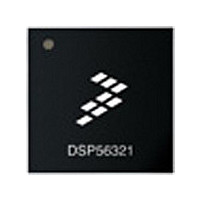
XC56309VL100A Freescale Semiconductor, XC56309VL100A Datasheet - Page 25

XC56309VL100A
Manufacturer Part Number
XC56309VL100A
Description
IC DSP 24BIT 100MHZ 196-MAPBGA
Manufacturer
Freescale Semiconductor
Series
DSP563xxr
Type
Fixed Pointr
Specifications of XC56309VL100A
Interface
Host Interface, SSI, SCI
Clock Rate
100MHz
Non-volatile Memory
ROM (576 B)
On-chip Ram
24kB
Voltage - I/o
3.30V
Voltage - Core
3.30V
Operating Temperature
-40°C ~ 100°C
Mounting Type
Surface Mount
Package / Case
196-MAPBGA
Device Core Size
24b
Format
Fixed Point
Clock Freq (max)
100MHz
Mips
100
Device Input Clock Speed
100MHz
Ram Size
102KB
Operating Supply Voltage (typ)
3.3V
Operating Supply Voltage (min)
3V
Operating Supply Voltage (max)
3.6V
Operating Temp Range
-40C to 100C
Operating Temperature Classification
Industrial
Mounting
Surface Mount
Pin Count
196
Package Type
MA-BGA
Lead Free Status / RoHS Status
Lead free / RoHS Compliant
Available stocks
Company
Part Number
Manufacturer
Quantity
Price
Company:
Part Number:
XC56309VL100A
Manufacturer:
Freescale Semiconductor
Quantity:
10 000
Company:
Part Number:
XC56309VL100AR2
Manufacturer:
Freescale Semiconductor
Quantity:
10 000
- Current page: 25 of 284
- Download datasheet (4Mb)
Signals/Connections
The DSP56309 input and output signals are organized into functional groups, as shown in Table
2-1 and illustrated in Figure 2-1. The DSP56309 operates from a 3 V supply; however, some of
the inputs can tolerate 5 V. A special notice for this feature is added to the signal descriptions of
those inputs.
Freescale Semiconductor
Power (V
Ground (GND)
Clock
PLL
Address bus
Data bus
Bus control
Interrupt and mode control
HI08
ESSI
SCI
Timer
OnCE/JTAG Port
Notes: 1.
5
2.
3.
4.
5.
CC
)
Port A signals define the external memory interface port, including the external address bus, data bus, and
control signals.
Port B signals are the HI08 port signals multiplexed with the GPIO signals.
Port C and D signals are the two ESSI port signals multiplexed with the GPIO signals.
Port E signals are the SCI port signals multiplexed with the GPIO signals.
The number of Ground signals listed are for the 144-pin TQFP package. For the 196-ball MAP-BGA package,
there are 66 GND connections.
Functional Group
Table 2-1. DSP56309 Functional Signal Groupings
DSP56309 User’s Manual, Rev. 1
Ports C and D
Port A
Port E
Port B2
1
4
3
Number of Signals
18
19
18
24
13
16
12
2
3
5
3
3
6
Table 2-2 on page -3
Table 2-3 on page -3
Table 2-4 on page -4
Table 2-5 on page -5
Table 2-6 on page -5
Table 2-7 on page -6
Table 2-8 on page -6
Table 2-9 on page -8
Table 2-11 on page -10
Table 2-12 on page -14
Table 2-13 on page -16
Table 2-14 on page -18
Table 2-15 on page -19
Table 2-16 on page -20
Description and Page
2
2-1
Related parts for XC56309VL100A
Image
Part Number
Description
Manufacturer
Datasheet
Request
R
Part Number:
Description:
Manufacturer:
Freescale Semiconductor, Inc
Datasheet:
Part Number:
Description:
Manufacturer:
Freescale Semiconductor, Inc
Datasheet:
Part Number:
Description:
Manufacturer:
Freescale Semiconductor, Inc
Datasheet:
Part Number:
Description:
Manufacturer:
Freescale Semiconductor, Inc
Datasheet:
Part Number:
Description:
Manufacturer:
Freescale Semiconductor, Inc
Datasheet:
Part Number:
Description:
Manufacturer:
Freescale Semiconductor, Inc
Datasheet:
Part Number:
Description:
Manufacturer:
Freescale Semiconductor, Inc
Datasheet:
Part Number:
Description:
Manufacturer:
Freescale Semiconductor, Inc
Datasheet:
Part Number:
Description:
Manufacturer:
Freescale Semiconductor, Inc
Datasheet:
Part Number:
Description:
Manufacturer:
Freescale Semiconductor, Inc
Datasheet:
Part Number:
Description:
Manufacturer:
Freescale Semiconductor, Inc
Datasheet:
Part Number:
Description:
Manufacturer:
Freescale Semiconductor, Inc
Datasheet:
Part Number:
Description:
Manufacturer:
Freescale Semiconductor, Inc
Datasheet:
Part Number:
Description:
Manufacturer:
Freescale Semiconductor, Inc
Datasheet:
Part Number:
Description:
Manufacturer:
Freescale Semiconductor, Inc
Datasheet:


