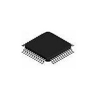
MC68908GZ8MFAE Freescale Semiconductor, MC68908GZ8MFAE Datasheet - Page 235

MC68908GZ8MFAE
Manufacturer Part Number
MC68908GZ8MFAE
Description
IC MCU 8BIT 8K FLASH 48-LQFP
Manufacturer
Freescale Semiconductor
Series
HC08r
Datasheet
1.MC68908GZ8CFJER.pdf
(314 pages)
Specifications of MC68908GZ8MFAE
Core Processor
HC08
Core Size
8-Bit
Speed
8MHz
Connectivity
CAN, LIN, SCI, SPI
Peripherals
LVD, POR, PWM
Number Of I /o
37
Program Memory Size
8KB (8K x 8)
Program Memory Type
FLASH
Ram Size
1K x 8
Voltage - Supply (vcc/vdd)
3 V ~ 5.5 V
Data Converters
A/D 8x10b
Oscillator Type
Internal
Operating Temperature
-40°C ~ 125°C
Package / Case
48-LQFP
Processor Series
M689xx
Core
HC08
Data Bus Width
8 bit
Data Ram Size
1 KB
Interface Type
SPI, SCI, CAN
Maximum Clock Frequency
8 MHz
Number Of Programmable I/os
37
Number Of Timers
2
Operating Supply Voltage
5.5 V
Maximum Operating Temperature
+ 125 C
Mounting Style
SMD/SMT
Development Tools By Supplier
FSICEBASE, M68CBL05AE, DEMO908GZ60E, M68EML08GZE
Minimum Operating Temperature
- 40 C
On-chip Adc
10 bit, 16 Channel
Lead Free Status / RoHS Status
Lead free / RoHS Compliant
Eeprom Size
-
Lead Free Status / Rohs Status
Details
- Current page: 235 of 314
- Download datasheet (5Mb)
17.4.2 Slave Mode
The SPI operates in slave mode when the SPMSTR bit is clear. In slave mode, the SPSCK pin is the input
for the serial clock from the master MCU. Before a data transmission occurs, the SS pin of the slave SPI
must be at logic 0. SS must remain low until the transmission is complete. See
In a slave SPI module, data enters the shift register under the control of the serial clock from the master
SPI module. After a byte enters the shift register of a slave SPI, it transfers to the receive data register,
and the SPRF bit is set. To prevent an overflow condition, slave software then must read the receive data
register before another full byte enters the shift register.
The maximum frequency of the SPSCK for an SPI configured as a slave is the bus clock speed (which is
twice as fast as the fastest master SPSCK clock that can be generated). The frequency of the SPSCK for
an SPI configured as a slave does not have to correspond to any SPI baud rate. The baud rate only
controls the speed of the SPSCK generated by an SPI configured as a master. Therefore, the frequency
of the SPSCK for an SPI configured as a slave can be any frequency less than or equal to the bus speed.
When the master SPI starts a transmission, the data in the slave shift register begins shifting out on the
MISO pin. The slave can load its shift register with a new byte for the next transmission by writing to its
transmit data register. The slave must write to its transmit data register at least one bus cycle before the
master starts the next transmission. Otherwise, the byte already in the slave shift register shifts out on the
MISO pin. Data written to the slave shift register during a transmission remains in a buffer until the end of
the transmission.
When the clock phase bit (CPHA) is set, the first edge of SPSCK starts a transmission. When CPHA is
clear, the falling edge of SS starts a transmission. See
17.5 Transmission Formats
During an SPI transmission, data is simultaneously transmitted (shifted out serially) and received (shifted
in serially). A serial clock synchronizes shifting and sampling on the two serial data lines. A slave select
line allows selection of an individual slave SPI device; slave devices that are not selected do not interfere
with SPI bus activities. On a master SPI device, the slave select line can optionally be used to indicate
multiple-master bus contention.
17.5.1 Clock Phase and Polarity Controls
Software can select any of four combinations of serial clock (SPSCK) phase and polarity using two bits
in the SPI control register (SPCR). The clock polarity is specified by the CPOL control bit, which selects
an active high or low clock and has no significant effect on the transmission format.
The clock phase (CPHA) control bit selects one of two fundamentally different transmission formats. The
clock phase and polarity should be identical for the master SPI device and the communicating slave
device. In some cases, the phase and polarity are changed between transmissions to allow a master
device to communicate with peripheral slaves having different requirements.
Freescale Semiconductor
SPSCK must be in the proper idle state before the slave is enabled to
prevent SPSCK from appearing as a clock edge.
Before writing to the CPOL bit or the CPHA bit, disable the SPI by clearing
the SPI enable bit (SPE).
MC68HC908GZ16 • MC68HC908GZ8 Data Sheet, Rev. 4
NOTE
NOTE
17.5 Transmission
Formats.
17.7.2 Mode Fault
Transmission Formats
Error.
235
Related parts for MC68908GZ8MFAE
Image
Part Number
Description
Manufacturer
Datasheet
Request
R
Part Number:
Description:
Manufacturer:
Freescale Semiconductor, Inc
Datasheet:
Part Number:
Description:
Manufacturer:
Freescale Semiconductor, Inc
Datasheet:
Part Number:
Description:
Manufacturer:
Freescale Semiconductor, Inc
Datasheet:
Part Number:
Description:
Manufacturer:
Freescale Semiconductor, Inc
Datasheet:
Part Number:
Description:
Manufacturer:
Freescale Semiconductor, Inc
Datasheet:
Part Number:
Description:
Manufacturer:
Freescale Semiconductor, Inc
Datasheet:
Part Number:
Description:
Manufacturer:
Freescale Semiconductor, Inc
Datasheet:
Part Number:
Description:
Manufacturer:
Freescale Semiconductor, Inc
Datasheet:
Part Number:
Description:
Manufacturer:
Freescale Semiconductor, Inc
Datasheet:
Part Number:
Description:
Manufacturer:
Freescale Semiconductor, Inc
Datasheet:
Part Number:
Description:
Manufacturer:
Freescale Semiconductor, Inc
Datasheet:
Part Number:
Description:
Manufacturer:
Freescale Semiconductor, Inc
Datasheet:
Part Number:
Description:
Manufacturer:
Freescale Semiconductor, Inc
Datasheet:
Part Number:
Description:
Manufacturer:
Freescale Semiconductor, Inc
Datasheet:
Part Number:
Description:
Manufacturer:
Freescale Semiconductor, Inc
Datasheet:


