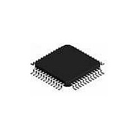
MC68908GZ8MFAE Freescale Semiconductor, MC68908GZ8MFAE Datasheet - Page 69

MC68908GZ8MFAE
Manufacturer Part Number
MC68908GZ8MFAE
Description
IC MCU 8BIT 8K FLASH 48-LQFP
Manufacturer
Freescale Semiconductor
Series
HC08r
Datasheet
1.MC68908GZ8CFJER.pdf
(314 pages)
Specifications of MC68908GZ8MFAE
Core Processor
HC08
Core Size
8-Bit
Speed
8MHz
Connectivity
CAN, LIN, SCI, SPI
Peripherals
LVD, POR, PWM
Number Of I /o
37
Program Memory Size
8KB (8K x 8)
Program Memory Type
FLASH
Ram Size
1K x 8
Voltage - Supply (vcc/vdd)
3 V ~ 5.5 V
Data Converters
A/D 8x10b
Oscillator Type
Internal
Operating Temperature
-40°C ~ 125°C
Package / Case
48-LQFP
Processor Series
M689xx
Core
HC08
Data Bus Width
8 bit
Data Ram Size
1 KB
Interface Type
SPI, SCI, CAN
Maximum Clock Frequency
8 MHz
Number Of Programmable I/os
37
Number Of Timers
2
Operating Supply Voltage
5.5 V
Maximum Operating Temperature
+ 125 C
Mounting Style
SMD/SMT
Development Tools By Supplier
FSICEBASE, M68CBL05AE, DEMO908GZ60E, M68EML08GZE
Minimum Operating Temperature
- 40 C
On-chip Adc
10 bit, 16 Channel
Lead Free Status / RoHS Status
Lead free / RoHS Compliant
Eeprom Size
-
Lead Free Status / Rohs Status
Details
- Current page: 69 of 314
- Download datasheet (5Mb)
4.5.1 PLL Control Register
The PLL control register (PCTL) contains the interrupt enable and flag bits, the on/off switch, the base
clock selector bit, and the VCO power-of-two range selector bits.
Freescale Semiconductor
NOTES:
Addr.
$003A
$003B
$0036
$0037
$0038
$0039
1. When AUTO = 0, PLLIE is forced clear and is read-only.
2. When AUTO = 0, PLLF and LOCK read as clear.
3. When AUTO = 1, ACQ is read-only.
4. When PLLON = 0 or VRS7:VRS0 = $0, BCS is forced clear and is read-only.
5. When PLLON = 1, the PLL programming register is read-only.
6. When BCS = 1, PLLON is forced set and is read-only.
PLL Multiplier Select High
PLL Multiplier Select Low
PLL VCO Select Range
PLL Bandwidth Control
Register Name
PLL Control Register
Address:
Reserved Register
Register (PBWC)
Register (PMSH)
Register (PMRS)
Reset:
Register (PMSL)
Read:
Write:
See page 69.
See page 71.
See page 72.
See page 73.
See page 73.
(PCTL)
$0036
PLLIE
Bit 7
0
Reset:
Reset:
Reset:
Reset:
Reset:
Reset:
MC68HC908GZ16 • MC68HC908GZ8 Data Sheet, Rev. 4
Read:
Read:
Read:
Read:
Read:
Read:
Write:
Write:
Write:
Write:
Write:
Write:
= Unimplemented
Figure 4-4. PLL Control Register (PCTL)
Figure 4-3. CGM I/O Register Summary
PLLF
6
0
PLLIE
AUTO
MUL7
VRS7
Bit 7
0
0
0
0
0
0
0
0
PLLON
5
1
= Unimplemented
LOCK
MUL6
VRS6
PLLF
6
0
0
0
0
1
1
0
0
BCS
4
0
PLLON
MUL5
VRS5
ACQ
5
1
0
0
0
0
0
0
0
R
R
3
0
MUL4
VRS4
BCS
R
4
0
0
0
0
0
0
0
0
0
= Reserved
= Reserved
R
2
0
MUL11
MUL3
VRS3
R
R
3
0
0
0
0
0
0
0
VPR1
1
0
MUL10
MUL2
VRS2
R
R
2
0
0
0
0
0
0
0
VPR0
Bit 0
0
VPR1
MUL9
MUL1
VRS1
R
1
0
0
0
0
0
0
0
CGM Registers
VPR0
MUL8
MUL0
VRS0
Bit 0
R
R
0
0
0
0
0
1
69
Related parts for MC68908GZ8MFAE
Image
Part Number
Description
Manufacturer
Datasheet
Request
R
Part Number:
Description:
Manufacturer:
Freescale Semiconductor, Inc
Datasheet:
Part Number:
Description:
Manufacturer:
Freescale Semiconductor, Inc
Datasheet:
Part Number:
Description:
Manufacturer:
Freescale Semiconductor, Inc
Datasheet:
Part Number:
Description:
Manufacturer:
Freescale Semiconductor, Inc
Datasheet:
Part Number:
Description:
Manufacturer:
Freescale Semiconductor, Inc
Datasheet:
Part Number:
Description:
Manufacturer:
Freescale Semiconductor, Inc
Datasheet:
Part Number:
Description:
Manufacturer:
Freescale Semiconductor, Inc
Datasheet:
Part Number:
Description:
Manufacturer:
Freescale Semiconductor, Inc
Datasheet:
Part Number:
Description:
Manufacturer:
Freescale Semiconductor, Inc
Datasheet:
Part Number:
Description:
Manufacturer:
Freescale Semiconductor, Inc
Datasheet:
Part Number:
Description:
Manufacturer:
Freescale Semiconductor, Inc
Datasheet:
Part Number:
Description:
Manufacturer:
Freescale Semiconductor, Inc
Datasheet:
Part Number:
Description:
Manufacturer:
Freescale Semiconductor, Inc
Datasheet:
Part Number:
Description:
Manufacturer:
Freescale Semiconductor, Inc
Datasheet:
Part Number:
Description:
Manufacturer:
Freescale Semiconductor, Inc
Datasheet:


