AD8353ACP-R2 Analog Devices Inc, AD8353ACP-R2 Datasheet - Page 13
AD8353ACP-R2
Manufacturer Part Number
AD8353ACP-R2
Description
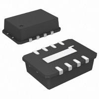
IC RF GAIN BLOCK 8-LFCSP
Manufacturer
Analog Devices Inc
Datasheet
1.AD8353ACPZ-REEL7.pdf
(16 pages)
Specifications of AD8353ACP-R2
Rohs Status
RoHS non-compliant
Current - Supply
35mA ~ 48mA
Frequency
1MHz ~ 2.7GHz
Gain
15.6dB
Noise Figure
6.8dB
P1db
6.3dBm
Package / Case
8-LFCSP
Rf Type
Cellular, LMDS, MMDS
Test Frequency
2.7GHz
Voltage - Supply
3V, 5V
Manufacturer's Type
Gain Amplifier
Number Of Channels
1
Supply Current
52@5VmA
Frequency (max)
2.7GHz
Operating Supply Voltage (min)
2.7V
Operating Supply Voltage (typ)
3/5V
Operating Supply Voltage (max)
5.5V
Package Type
LFCSP EP
Mounting
Surface Mount
Pin Count
8
Noise Figure (typ)
7.1@2700MHzdB
Operating Temp Range
-40C to 85C
Operating Temperature Classification
Industrial
Lead Free Status / Rohs Status
Not Compliant
Other names
AD8353ACP-R2CT


THEORY OF OPERATION
The AD8353 is a 2-stage, feedback amplifier employing both
shunt-series and shunt-shunt feedback. The first stage is
degenerated and resistively loaded and provides approximately
10 dB of gain. The second stage is a PNP-NPN Darlington
output stage, which provides another 10 dB of gain. Series-
shunt feedback from the emitter of the output transistor sets the
input impedance to 50 Ω over a broad frequency range. Shunt-
shunt feedback from the amplifier output to the input of the
Darlington stage helps to set the output impedance to 50 Ω. The
amplifier can be operated from a 3 V supply by adding a choke
inductor from the amplifier output to VPOS. Without this
choke inductor, operation from a 5 V supply is also possible.
BASIC CONNECTIONS
The AD8353 RF gain block is a fixed gain amplifier with
single-ended input and output ports whose impedances are
nominally equal to 50 Ω over the frequency range 1 MHz to
2.7 GHz. Consequently, it can be directly inserted into a 50 Ω
system with no impedance matching circuitry required.
The input and output impedances are sufficiently stable vs.
variations in temperature and supply voltage that no impedance
matching compensation is required. A complete set of
scattering parameters is available at www.analog.com.
The input pin (RFIN) is connected directly to the base of the first
amplifier stage, which is internally biased to approximately 1 V;
therefore, a dc blocking capacitor should be connected between the
source that drives the AD8353 and the input pin, RFIN.
Rev. C | Page 13 of 16
It is critical to supply very low inductance ground connections
to the ground pins (Pin 1, Pin 4, Pin 5, and Pin 8) as well as to
the backside exposed paddle. This ensures stable operation.
The AD8353 is designed to operate over a wide supply voltage
range, from 2.7 V to 5.5 V. The output of the part, RFOUT, is
taken directly from the collector of the output amplifier stage.
This node is internally biased to approximately 2.2 V when the
supply voltage is 5 V. Consequently, a dc blocking capacitor
should be connected between the output pin, RFOUT, and the
load that it drives. The value of this capacitor is not critical, but
it should be 100 pF or larger.
When the supply voltage is 3 V, it is recommended that an
external RF choke be connected between the supply voltage
and the output pin, RFOUT. This increases the dc voltage
applied to the collector of the output amplifier stage, which
improves performance of the AD8353 to be very similar to the
performance produced when 5 V is used for the supply voltage.
The inductance of the RF choke should be approximately
100 nH, and care should be taken to ensure that the lowest
series self-resonant frequency of this choke is well above the
maximum frequency of operation for the AD8353. For lower
frequency operation, use a higher value inductor.
Bypass the supply voltage input, VPOS, using a large value
capacitance (approximately 0.47 μF or larger) and a smaller,
high frequency bypass capacitor (approximately 100 pF)
physically located close to the VPOS pin.
The recommended connections and components are shown in
Figure 40.
AD8353
Related parts for AD8353ACP-R2
Image
Part Number
Description
Manufacturer
Datasheet
Request
R

Part Number:
Description:
250 MHz, Voltage Output 4-Quadrant Multiplier
Manufacturer:
Analog Devices
Datasheet:

Part Number:
Description:
±1.7g Dual-Axis IMEMS Accelerometer Evaluation Board
Manufacturer:
Analog Devices Inc
Datasheet:

Part Number:
Description:
Inertial Sensor Evaluation System
Manufacturer:
Analog Devices Inc
Datasheet:
Part Number:
Description:
Manufacturer:
Analog Devices Inc
Datasheet:
Part Number:
Description:
Manufacturer:
Analog Devices Inc
Datasheet:
Part Number:
Description:
Manufacturer:
Analog Devices Inc
Datasheet:
Part Number:
Description:
Manufacturer:
Analog Devices Inc
Datasheet:
Part Number:
Description:
Manufacturer:
Analog Devices Inc
Datasheet:
Part Number:
Description:
Manufacturer:
Analog Devices Inc
Datasheet:
Part Number:
Description:
Manufacturer:
Analog Devices Inc
Datasheet:
Part Number:
Description:
Manufacturer:
Analog Devices Inc
Datasheet:
Part Number:
Description:
Manufacturer:
Analog Devices Inc
Datasheet:
Part Number:
Description:
Manufacturer:
Analog Devices Inc
Datasheet: