EVB71102B-418-FSK-C Melexis Inc, EVB71102B-418-FSK-C Datasheet
EVB71102B-418-FSK-C
Specifications of EVB71102B-418-FSK-C
EVB71102-418-FSK
EVB71102-418F
EVB71102-418F
EVB71102B-418FSKC


Related parts for EVB71102B-418-FSK-C


EVB71102B-418-FSK-C Summary of contents
Page 1
Features Double-conversion superhet architecture for high degree of image rejection FSK demodulation with phase-coincidence demodulator Low current consumption in active mode and very low standby current Switchable LNA gain for improved dynamic range RSSI allows signal strength indication and ASK ...
Page 2
Document Content 1 Theory of Operation ...................................................................................................3 1.1 General ............................................................................................................................. 3 1.2 EVB Technical Data Overview ......................................................................................... 3 1.3 Block Diagram .................................................................................................................. 4 1.4 Mode Configurations ........................................................................................................ 4 1.5 LNA GAIN Control ............................................................................................................ 4 1.6 Frequency Planning.......................................................................................................... 4 1.6.1 Selected ...
Page 3
Theory of Operation 1.1 General With the TH71102 receiver chip, various circuit configurations can be arranged in order to meet a number of different customer requirements. For FSK reception the IF tank used in the phase coincidence demodulator can ...
Page 4
Block Diagram MIX1 IN_LNA LNA 31 LO1 DIV8 VCO1 32 30 1.4 Mode Configurations ENRX 0 1 Note: ENRX are pulled down internally 1.5 LNA GAIN Control V GAIN_LNA < 0.8 V HIGH GAIN ...
Page 5
By configuring the TH71102 for double conversion and using its internal PLL synthesizer with fixed feedback divider ratios (DIV_8) and (DIV_2), four types of down-conversion are possible: low-side injection of LO1 and LO2 ...
Page 6
Application Circuits 2.1 FSK Application Circuit 2.1.1 Circuit Diagram for FSK Reception GND RO VCC VCC ENRX GND IN_LNA 1 6 SAWFIL Circuit Features • Tolerates input frequency variations • Well-suited for NRZ, Manchester and similar ...
Page 7
Board Component Values for FSK Value Part Size @ 315 MHz C1 0805 0603 0603 6 0603 2 0603 0603 33 nF C10 0603 1 nF ...
Page 8
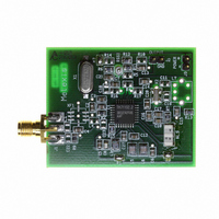
Component Arrangement Top Side for FSK Reception Board size is 42.7mm x 37.5mm Melexis RF_input IN_LNA EVB711XX_4 39012 71102 01 Rev. 012 Evaluation Board Description 1 C15 R5 XTAL CB2 TH71102 CB1 ...
Page 9
ASK Application Circuit 2.2.1 Circuit Diagram for ASK Reception GND RO VCC VCC ENRX GND IN_LNA 6 1 SAWFIL 39012 71102 01 Rev. 012 Evaluation Board Description 1 2 C16 C17 XTAL C1 25 VEE C_RO ...
Page 10
Board Component Values for ASK Value Part Size @ 315 MHz C1 0805 0603 0603 6 0603 2 0603 0603 33 nF C10 0603 1 nF ...
Page 11
Component Arrangement Top Side for ASK Reception Board size is 42.7mm x 37.5mm Melexis RF_input IN_LNA EVB711XX_4 39012 71102 01 Rev. 012 Evaluation Board Description XTAL CB2 TH71102 CB1 L3 C6 CB8 ...
Page 12
Evaluation Board Layouts Board layout data in Gerber format is available, board size is 37.5mm x 42.7mm. OUT_OA RSSI OUTP OUTN RO ENRX PCB top view 39012 71102 01 Rev. 012 315/433MHz Receiver Evaluation Board Description PCB bottom view ...
Page 13
Package Description The device TH71102 is RoHS compliant 12° Fig. 2: LQFP32 (Low profile Quad Flat Package) All Dimension in mm, coplanaríty < 0.1mm E1 min 7.00 9.00 max All Dimension ...
Page 14
Disclaimer 1) The information included in this documentation is subject to Melexis intellectual and other property rights. Reproduction of information is permissible only if the information will not be altered and is accom- panied by all associated conditions, limitations ...