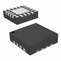
SI4312-B10-GM Silicon Laboratories Inc, SI4312-B10-GM Datasheet - Page 13

SI4312-B10-GM
Manufacturer Part Number
SI4312-B10-GM
Description
IC RX OOK 315/434MHZ 20VQFN
Manufacturer
Silicon Laboratories Inc
Series
EZRadio®r
Type
ISM Receiverr
Specifications of SI4312-B10-GM
Package / Case
20-VQFN
Frequency
315MHz, 434MHz
Sensitivity
-110dBm
Data Rate - Maximum
10 kBaud
Modulation Or Protocol
OOK
Applications
Garage Openers, RKE, Security Alarms
Data Interface
PCB, Surface Mount
Antenna Connector
PCB, Surface Mount
Voltage - Supply
2.7 V ~ 3.6 V
Operating Temperature
-40°C ~ 85°C
Operating Frequency
315 MHz to 434 MHz
Operating Supply Voltage
2.7 V to 3.6 V
Maximum Operating Temperature
+ 95 C
Minimum Operating Temperature
- 45 C
Mounting Style
SMD/SMT
Supply Current
20 mA
Lead Free Status / RoHS Status
Lead free / RoHS Compliant
Features
-
Memory Size
-
Current - Receiving
-
Lead Free Status / Rohs Status
Lead free / RoHS Compliant
Other names
336-1977-5
Si4312
3.9. Crystal Oscillator
An on-board crystal oscillator is used to generate a 16 MHz reference clock for the Si4312. This reference
frequency is required for proper operation of the Si4312 and is used for calibration of the on-chip VCO and other
timing references. No external load capacitors are required to set the 16 MHz reference frequency if the
recommended crystal load capacitor is around 14 pF, assuming the effective board capacitance between pins
XTL1 and XTL2 is 3 pF and the chip input capacitance on pins XTL1 or XTL2 is 11 pF. Refer to Table 6, “Crystal
Characteristics,” on page 6 for board capacitance and frequency tolerance information. The frequency tolerance of
the crystal should be chosen such that the received signal is within the IF bandwidth of the Si4312 receiver.
Additionally, the Si4312 can be driven by an external 16 MHz reference clock. The clock signal can be applied to
either the XTL1 or XTL2 inputs. When the 16 MHz reference clock is applied to one of the inputs, the other crystal
input pin must be floating.
3.10. Reset Pin
Driving the RST pin (pin 4) low will disable the Si4312 and place the device into reset mode. All active blocks in the
device are powered off in this mode, bringing the current consumption to less than 10 uA. The Si4312 is enabled
by driving the RST pin (pin 4) to VDD. Refer to Table 4 "Reset Timing Characteristics" for the reset timing
requirements. The chip requires about 500 ms to go from reset to active mode. The Si4312 can output invalid data
during the 500 ms turn-on time.
Rev. 0.5
13


