MICRF500BLQTR Micrel Inc, MICRF500BLQTR Datasheet - Page 15
MICRF500BLQTR
Manufacturer Part Number
MICRF500BLQTR
Description
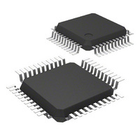
TXRX UHF 700-1100MHZ 44-LQFP
Manufacturer
Micrel Inc
Datasheet
1.MICRF500EVAL1.pdf
(18 pages)
Specifications of MICRF500BLQTR
Frequency
700MHz Center
Data Rate - Maximum
128kBaud
Modulation Or Protocol
FSK
Applications
Remote Control, Remote Metering
Power - Output
10dBm
Sensitivity
-104dBm
Voltage - Supply
2.5 V ~ 3.4 V
Current - Receiving
12mA
Current - Transmitting
50mA
Data Interface
PCB, Surface Mount
Antenna Connector
PCB, Surface Mount
Operating Temperature
-40°C ~ 85°C
Package / Case
44-LQFP
Lead Free Status / RoHS Status
Contains lead / RoHS non-compliant
Memory Size
-


March 2003
MICRF500
Name
A1
A0
N1
N0
M1
M0
RxFilt
Pa2
Pa1
Pa0
Gc
ByLNA
Ref6
Ref5
Ref4
Ref3
Ref2
Ref1
Ref0
Cpmp1
Cpmp0
Fc1
Fc0
OutS2
OutS1
OutS0
Mod1
Mod0
RT
Pu
frequency divider N1, 12 bits
frequency divider N0, 12 bits
frequency divider M1, 10 bits
frequency divider M0, 10 bits
1=external capacitor for filtering of Rx data signal
gain control in power amplifier buffer: 1=high gain
gain control in preamplifier in receiver: 1=high gain
Active RC-filter settings
I- and Q-channel
sk:_*:Sallen-Key filter output, gm_*:gyrator filter output, lim_*:limiter output, *_div:frequency divider output
(for testing). 110 is for dual-loop filter applications, see “Modulation Outside PLL, Dual-Loop Filters.”
Mod1 = 1, Mod0 = 0: FSK modulation by switching between the two sets of dividers
Mod1 = 1, Mod0 = 1: FSK modulation by adding/subtracting 1 to divider A1: f
0 = receive mode 1 = transmit mode
Description
frequency divider A1, 6 bits
frequency divider A0, 6 bits
gain setting in power amplifier
pa2, pa1, pa0 = 0 : lowest output power
pa2, pa1, pa0 = 1 : highest output power
1 = the LNA is bypassed
reference settings in lock detector
all 0’s: highest reference
all 1’s: lowest reference
charge pump setting:
output select
Mod1 = 0, Mod0 = 0: FSK modulation can be applied to the VCO
Mod1 = 0, Mod0 = 1: FSK modulation can be applied to the VCO: open loop modulation
1 = power up, 0 = power down (When Pu=1, power down is controlled by PuExt)
Cpmp1=0, Cpmp0=0 : ±125µA
Cpmp1=0, Cpmp0=1 : ±500µA
Cpmp1=1, Cpmp0=0 : controlled by LockDet (LD) LD=0: ±500µA, LD=1: ±125µA
Cpmp1=1, Cpmp0=1 : same as previous in Tx. In Rx the current is ±500µA.
Fc1=0, Fc0=0 : 10kHz
Fc1=0, Fc0=1 : 30kHz
OutS2 OutS1
0
0
0
0
0
0
1
1
Table 2. Bit Description
OutS0 IchOut
0
1
0
1
Fc1=1, Fc0=0 : 60kHz
Fc1=1, Fc0=1 : 200kHz
high Z
sk_ich
gm_ich
lim_ich
15
QchOut
high Z
sk_qch
gm_qch
lim_qch
OutS2
1
1
1
1
deviation
OutS1
0
0
1
1
= f
comparison
OutS0
0
1
0
1
IchOut
lim_qch
gm_ich
high Z
N_div
MICRF500
QchOut
gm_qch
lim_ich
Dual LF
M_div
Micrel
Related parts for MICRF500BLQTR
Image
Part Number
Description
Manufacturer
Datasheet
Request
R

Part Number:
Description:
Manufacturer:
Micrel Inc
Datasheet:
Part Number:
Description:
Manufacturer:
Micrel Inc
Datasheet:
Part Number:
Description:
Manufacturer:
Micrel Inc
Datasheet:
Part Number:
Description:
Manufacturer:
Micrel Inc
Datasheet:
Part Number:
Description:
Manufacturer:
Micrel Inc
Datasheet:
Part Number:
Description:
Manufacturer:
Micrel Inc
Datasheet:
Part Number:
Description:
Manufacturer:
Micrel Inc
Datasheet:
Part Number:
Description:
Manufacturer:
Micrel Inc
Datasheet:
Part Number:
Description:
Manufacturer:
Micrel Inc
Datasheet:
Part Number:
Description:
Manufacturer:
Micrel Inc
Datasheet:
Part Number:
Description:
Manufacturer:
Micrel Inc
Datasheet:
Part Number:
Description:
Manufacturer:
Micrel Inc
Datasheet:
Part Number:
Description:
Manufacturer:
Micrel Inc
Datasheet:
Part Number:
Description:
Manufacturer:
Micrel Inc
Datasheet: