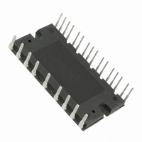
STGIPS10K60A STMicroelectronics, STGIPS10K60A Datasheet
STGIPS10K60A
Specifications of STGIPS10K60A
Available stocks


Related parts for STGIPS10K60A


STGIPS10K60A Summary of contents
Page 1
... Home appliances, such as washing machines, refrigerators, air conditioners Description The STGIPS10K60A intelligent power module provides a compact, high performance AC motor drive for a simple and rugged design. It mainly targets low power inverters for applications such as home appliances and air conditioners. It ...
Page 2
... Internal block diagram and pin configuration . . . . . . . . . . . . . . . . . . . . 3 2 Electrical ratings . . . . . . . . . . . . . . . . . . . . . . . . . . . . . . . . . . . . . . . . . . . . 5 2.1 Absolute maximum ratings . . . . . . . . . . . . . . . . . . . . . . . . . . . . . . . . . . . . . 5 2.2 Thermal data . . . . . . . . . . . . . . . . . . . . . . . . . . . . . . . . . . . . . . . . . . . . . . . 6 3 Electrical characteristics . . . . . . . . . . . . . . . . . . . . . . . . . . . . . . . . . . . . . 7 3.1 Control part . . . . . . . . . . . . . . . . . . . . . . . . . . . . . . . . . . . . . . . . . . . . . . . . 9 3.1.1 4 Applications information . . . . . . . . . . . . . . . . . . . . . . . . . . . . . . . . . . . . 12 4.1 Recommendations . . . . . . . . . . . . . . . . . . . . . . . . . . . . . . . . . . . . . . . . . . 13 5 Package mechanical data . . . . . . . . . . . . . . . . . . . . . . . . . . . . . . . . . . . . 14 6 Revision history . . . . . . . . . . . . . . . . . . . . . . . . . . . . . . . . . . . . . . . . . . . 16 2/17 NTC thermistor . . . . . . . . . . . . . . . . . . . . . . . . . . . . . . . . . . . . . . . . . . . 10 Doc ID 15587 Rev 5 STGIPS10K60A ...
Page 3
... STGIPS10K60A 1 Internal block diagram and pin configuration Figure 1. Internal block diagram Pin in 1 OUT U V boot boot HIN OUT V V boot boot HIN V OUT W V boot boot HIN Pin in 16 Internal block diagram and pin configuration LIN V boot boot HIN HVG ...
Page 4
... High side logic input for W phase W T NTC thermistor terminal NTC thermistor terminal Negative DC input for W phase phase output P Positive DC input N Negative DC input for V phase phase output P Positive DC input N Negative DC input for U phase phase output P Positive DC input Doc ID 15587 Rev 5 STGIPS10K60A Description ...
Page 5
... STGIPS10K60A 2 Electrical ratings 2.1 Absolute maximum ratings Table 3. Inverter part Symbol V Supply voltage applied between Supply voltage (surge) applied between PN(surge Collector emitter voltage (V CES Each IGBT continuous collector current at (2) ± 25°C C (3) Each IGBT pulsed collector current ± Each IGBT total dissipation at T ...
Page 6
... Operating junction temperature j 2.2 Thermal data Table 6. Thermal data Symbol Thermal resistance junction-case single IGBT max. R thj-c Thermal resistance junction-case single diode max. 6/17 Parameter Parameter Doc ID 15587 Rev 5 STGIPS10K60A Value Unit 2500 V -40 to 125 °C Value Unit 3.8 °C/W 5.5 °C/W ...
Page 7
... STGIPS10K60A 3 Electrical characteristics (T = 25°C unless otherwise specified). j Table 7. Inverter part Symbol Collector-emitter V CE(sat) saturation voltage Collector-cut off current I CES ( Diode forward voltage F Inductive load switching time and energy t Turn-on time on t Crossover time (on) c(on) t Turn-off time off t Crossover time (off) ...
Page 8
... Electrical characteristics Figure 3. Switching time test circuit Figure 4. Switching time definition 8/17 Doc ID 15587 Rev 5 STGIPS10K60A ...
Page 9
... STGIPS10K60A 3.1 Control part Table 8. Low supply voltage Symbol V Under voltage turn on threshold CCth1 V Under voltage turn off threshold CCth2 V Under voltage hystereses CChys Under voltage quiescent supply I qccu current I Quiescent current qcc R Bootstrap driver on resistance DS(on) Table 9. Bootstrap supply Symbol ...
Page 10
... B-constant T Operating temperature Equation 1: resistance variation vs temperature Figure 5. Typical NTC resistance vs temperature 10/17 Parameter Test conditions ⎛ – B ⎝ ⋅ Doc ID 15587 Rev 5 STGIPS10K60A Min. Typ. Max. Unit. = 25° 125°C 300 = 25°C 3435 -40 125 ⎞ 1 ------------ - ⎠ 298k kΩ Ω k °C ...
Page 11
... STGIPS10K60A Figure 6. Maximum I C(RMS) switching frequency I C (RMS) ( 300 V, Modulation index = 0 0. 125 ° SINE ° ° 100 Simulated curves refer to typical IGBT parameters and maximum R Figure 8. Dead time and interlocking definition LIN H IN LVG HVG Minimum recommended dead time (DT) between low and high side logic input: 1 µs. ...
Page 12
... Applications information 4 Applications information Figure 9. Typical application circuit 12/17 Doc ID 15587 Rev 5 STGIPS10K60A ...
Page 13
... STGIPS10K60A 4.1 Recommendations ● To prevent the input signals oscillation, the wiring of each input should be as short as possible. ● By integrating an application specific type HVIC inside the module, direct coupling to MCU terminals without any opto-coupler is possible. ● Each capacitor should be located as nearby the pins of IPM as possible. ...
Page 14
... Doc ID 15587 Rev 5 STGIPS10K60A ® Max. 44.8 1.75 2 39.8 22.4 12.25 25.63 5.8 7.4 12.1 2.75 4 5.1 6.9 1.2 0.7 2.15 0.7 ...
Page 15
... STGIPS10K60A Figure 10. SDIP-25L package mechanical data Doc ID 15587 Rev 5 Package mechanical data 8154676_F 15/17 ...
Page 16
... Inverter part, Figure 5: Typical NTC resistance vs Figure 6: Maximum IC(RMS) current vs. switching Figure 7: Maximum IC(RMS) current vs. fSINE (1) Section 5: Package mechanical Table 7: Inverter Updated 5 Minor text changes to improve readability. Doc ID 15587 Rev 5 STGIPS10K60A Changes Figure 7. Table 7. Table 12: and conditions. system, Table 6: Thermal data, ...
Page 17
... STGIPS10K60A Information in this document is provided solely in connection with ST products. STMicroelectronics NV and its subsidiaries (“ST”) reserve the right to make changes, corrections, modifications or improvements, to this document, and the products and services described herein at any time, without notice. All ST products are sold pursuant to ST’s terms and conditions of sale. ...