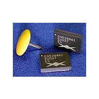
EN5364QI-E Enpirion, EN5364QI-E Datasheet - Page 6

EN5364QI-E
Manufacturer Part Number
EN5364QI-E
Description
Power Management Modules & Development Tools Eval Bd 6A Syn Buck PWM DC-DC Converter
Manufacturer
Enpirion
Type
DC/DC Switching Converters, Regulators & Controllersr
Datasheet
1.EN5364QI-E.pdf
(10 pages)
Specifications of EN5364QI-E
Input Voltage
2.375 V to 6.6 V
Output Voltage
0.6 V
Maximum Operating Temperature
+ 85 C
Minimum Operating Temperature
- 40 C
Product
Power Management Modules
For Use With/related Products
EN5364QI
Lead Free Status / RoHS Status
Lead free / RoHS Compliant
Available stocks
Company
Part Number
Manufacturer
Quantity
Price
Company:
Part Number:
EN5364QI-E
Manufacturer:
ST
Quantity:
34 000
Company:
Part Number:
EN5364QI-E
Manufacturer:
Enpirion
Quantity:
135
STEP 7: Phase Lock
device. Connect a pulse generator (properly terminated and output disabled)
signal between S_IN and GND. Set the pulse amplitude to swing from 0 to 2.5
volts. Set the pulse frequency to 4MHz. Connect oscilloscope probes to S_IN &
S_OUT. Power up device. Enable device. Note S_OUT – it is the free running
switching frequency. Now enable the pulse generator output. S_OUT should be
locked to S_IN with a fixed delay (depending on the value of the S_Delay
resistor.) Sweep the clock frequency between 3.6 and 4.4 MHz and note the lock
range at both extremes.
You may next wish to observe the delay as a function of S_Delay resistor.
ALWAYS power down device before changing board level components!
STEP 8: Pre-Bias Operation
Power down device. Set EN_PB jumper to logical “1.” Connect a pulse generator
(output disabled) signal to the middle pin of ENA and Ground. Set the pulse
amplitude to swing from 0 to 2.5 volts. Set the pulse period to 10msec., duty
cycle to 50% and fast transition (<1usec.) Hook up oscilloscope probes to ENA,
SS, POK and VOUT with clean ground returns. Connect a power supply (set
desired voltage but output disabled) to TP18 (BF_IN.) D2 is a diode connecting
BF_IN to VOUT. Turn the back feed supply on. VOUT will charge to BF_IN minus
a diode drop. Set the output voltage to a level greater than the back feed voltage.
Enable pulse generator output. Observe the output voltage and SS voltage in
relation to the Enable pulse. Sweep the back feed voltage up and down but
always less than VOUT and note device operation.
MAR-1
Float
Float
Float
High
High
High
Low
Low
Low
Table-1 : Margin Block Truth Table
– Disable device by moving ENA jumper. Power down the
EN5364QI-EN5394QI Evaluation Board Application Note
– Disable device by removing Enable jumper.
MAR-2
Float
Float
Float
High
High
High
Low
Low
Low
Page 6 of 10
Output Modulation
0%, Delay Bypass
Reserved
+2.5%
-2.5%
+10%
-10%
+5%
-5%
0%
November 2009 V_3


