NCP5010EVB ON Semiconductor, NCP5010EVB Datasheet - Page 7
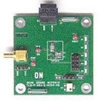
NCP5010EVB
Manufacturer Part Number
NCP5010EVB
Description
Power Management Modules & Development Tools EVAL BRD FOR NCP5010FCT1G
Manufacturer
ON Semiconductor
Datasheet
1.NCP5010EVB.pdf
(11 pages)
Specifications of NCP5010EVB
For Use With/related Products
NCP5010
Lead Free Status / RoHS Status
Lead free / RoHS Compliant


INPUT and OUTPUT POWER
SWITCHES SETUP
Symbol
Symbol
J1−1
J1−2
J2−1
J2−2
J6
J4
J3
This is the positive connection for power supply. The leads to the input supply should be twisted and kept as short
as possible.
This is the return connection for the power supply
Ground clip
Ground of the load connection
This is the output positive connection for the DC/DC boost converter
CTRL / Enable:
To enable the boost converter connect a shorting jumper between J4−1 and J4−2
Voltage Selection:
This jumper allows to select two different output voltage:
Shorting jumper between J6−2 and J6−3 give a fixed output voltage setup by R2/R4.
Shorting jumper between J6−1 and J6−2 R3 allow adjusting the output voltage.
NCP5010EVB/D
http://onsemi.com
7
Switch Descriptions
Switch Descriptions
Related parts for NCP5010EVB
Image
Part Number
Description
Manufacturer
Datasheet
Request
R

Part Number:
Description:
Boost Converter
Manufacturer:
ON Semiconductor
Datasheet:
Part Number:
Description:
ON Semiconductor [VOLTAGE REGULATOR]
Manufacturer:
ON Semiconductor
Datasheet:
Part Number:
Description:
357-036-542-201 CARDEDGE 36POS DL .156 BLK LOPRO
Manufacturer:
ON Semiconductor
Datasheet:
Part Number:
Description:
357-036-542-201 CARDEDGE 36POS DL .156 BLK LOPRO
Manufacturer:
ON Semiconductor
Datasheet:
Part Number:
Description:
357-036-542-201 CARDEDGE 36POS DL .156 BLK LOPRO
Manufacturer:
ON Semiconductor
Datasheet:
Part Number:
Description:
357-036-542-201 CARDEDGE 36POS DL .156 BLK LOPRO
Manufacturer:
ON Semiconductor
Datasheet:
Part Number:
Description:
357-036-542-201 CARDEDGE 36POS DL .156 BLK LOPRO
Manufacturer:
ON Semiconductor
Datasheet:
Part Number:
Description:
357-036-542-201 CARDEDGE 36POS DL .156 BLK LOPRO
Manufacturer:
ON Semiconductor
Datasheet:
Part Number:
Description:
357-036-542-201 CARDEDGE 36POS DL .156 BLK LOPRO
Manufacturer:
ON Semiconductor
Datasheet:
Part Number:
Description:
357-036-542-201 CARDEDGE 36POS DL .156 BLK LOPRO
Manufacturer:
ON Semiconductor
Datasheet:
Part Number:
Description:
357-036-542-201 CARDEDGE 36POS DL .156 BLK LOPRO
Manufacturer:
ON Semiconductor
Datasheet:
Part Number:
Description:
357-036-542-201 CARDEDGE 36POS DL .156 BLK LOPRO
Manufacturer:
ON Semiconductor
Datasheet:
Part Number:
Description:
Manufacturer:
ON Semiconductor
Datasheet:
Part Number:
Description:
Manufacturer:
ON Semiconductor
Datasheet: