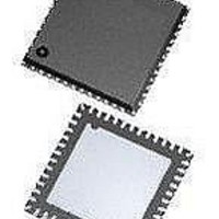
ASD5020L640INT Arctic Silicon Devices, ASD5020L640INT Datasheet - Page 24

ASD5020L640INT
Manufacturer Part Number
ASD5020L640INT
Description
ADC (A/D Converters) Mul-Md 12bit/640MSPS 8-bit 1000 MSPS ADC
Manufacturer
Arctic Silicon Devices
Datasheet
1.ASD5020L640INT.pdf
(34 pages)
Specifications of ASD5020L640INT
Number Of Converters
1
Number Of Adc Inputs
2
Conversion Rate
640 MSPs
Resolution
12 bit
Snr
70 dB
Voltage Reference
1 V
Supply Voltage (max)
2 V
Supply Voltage (min)
1.7 V
Maximum Power Dissipation
490 mW
Maximum Operating Temperature
+ 85 C
Mounting Style
SMD/SMT
Package / Case
QFN-48
Input Voltage
1.8 V
Minimum Operating Temperature
- 40 C
Lead Free Status / RoHS Status
Lead free / RoHS Compliant
Preliminary Product Specification
LVDS Drive Strength Programmability
The current delivered by the LVDS output drivers can be configured as shown in table 19. The default current is 3.5mA,
which is what the LVDS standard specifies.
Setting the ilvds_lclk<2:0> register controls the current drive strength of the LVDS clock output on the LCLKP and
LCLKN pins.
Setting the ilvds_frame<2:0> register controls the current drive strength of the frame clock output on the FCLKP and
FCLKN pins.
Setting the ilvds_dat<2:0> register controls the current drive strength of the data outputs on the D[8:1]P and D[8:1]N
pins.
LVDS Internal Termination Programmability
The off-chip load on the LVDS buffers may represent a characteristic impedance that is not perfectly matched with the
PCB traces. This may result in reflections back to the LVDS outputs and loss of signal integrity. This effect can be
mitigated by enabling an internal termination between the positive and negative outputs of each LVDS buffer. Internal
termination mode can be selected by setting the en_lvds_term bit to '1'. Once this bit is set, the internal termination
values for the bit clock, frame clock, and data buffers can be independently programmed using sets of three bits. Table
20 shows how the internal termination of the LVDS buffers are programmed. The values are typical values and can vary
by up to ±20% from device to device and across temperature.
ASD5020
ilvds_lclk<2:0>
ilvds_frame<2:0>
ilvds_dat<2:0>
en_lvds_term
term_lclk<2:0>
term_frame<2:0>
term_dat<2:0>
Name
Name
LVDS current drive programmability
for LCLKP and LCLKN pins.
LVDS current drive programmability
for FCLKP and FCLKN pins.
LVDS current drive programmability
for output data pins.
Enables internal termination for LVDS
buffers.
Programmable termination for LCLKN
and LCLKP buffers.
Programmable termination for FCLKN
and FCLKP buffers.
Programmable termination for output
data buffers.
Description
Description
Table 19: LVDS output drive strength for LCLK, FCLK and data
ilvds_*<2:0>
000
001
010
011
100
101
110
111
Termination disabled
Termination disabled
Termination disabled
Termination disabled
rev 2.0, 2010.11.08
3.5 mA drive
3.5 mA drive
3.5 mA drive
Default
Default
Page 24 of 34
LVDS drive strength
D15 D14D13D12D11D10 D9 D8 D7 D6 D5 D4 D3 D2 D1 D0
D15 D14D13D12D11D10 D9 D8 D7 D6 D5 D4 D3 D2 D1 D0
3.5 mA (default)
2.5 mA
1.5 mA (RSDS)
0.5 mA
7.5 mA
6.5 mA
5.5 mA
4.5 mA
X
1
1
1
X X X
X X X
X X X
X X X
High Speed Mode
X X X
X X X
Address
Address
0x12
Hex
0x11
Hex


