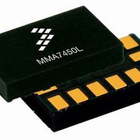
MMA7455LT Freescale Semiconductor, MMA7455LT Datasheet - Page 16

MMA7455LT
Manufacturer Part Number
MMA7455LT
Description
Board Mount Accelerometers 3-AXIS DIGITAL 2 4 8G
Manufacturer
Freescale Semiconductor
Datasheet
1.MMA7455LT.pdf
(35 pages)
Specifications of MMA7455LT
Sensing Axis
X, Y, Z
Acceleration
2 g, 4 g, 8 g
Supply Voltage (max)
3.6 V
Supply Voltage (min)
2.4 V
Supply Current
400 uA
Maximum Operating Temperature
+ 85 C
Minimum Operating Temperature
- 40 C
Sensitivity
64 LSB/g
Package / Case
LGA-14
Output Type
Digital
Acceleration Range
± 2g, ± 4g, ± 8g
No. Of Axes
3
Sensor Case Style
LGA
No. Of Pins
14
Supply Voltage Range
2.4V To 3.6V
Operating Temperature Range
-40°C To +85°C
Filter Terminals
SMD
Rohs Compliant
Yes
Ic Interface Type
I2C, SPI
Lead Free Status / RoHS Status
Lead free / RoHS Compliant
Available stocks
Company
Part Number
Manufacturer
Quantity
Price
Company:
Part Number:
MMA7455LT
Manufacturer:
FREESCALE
Quantity:
18 300
Part Number:
MMA7455LT
Manufacturer:
FREESCALE
Quantity:
20 000
Detecting Interrupts
LDX
1: Level detection event is detected on X-axis
0: Level detection event is not detected on X-axis
LDY
1: Level detection event is detected on Y-axis
0: Level detection event is not detected on Y-axis
LDZ
1: Level detection event is detected on Z-axis
0: Level detection event is not detected on Z-axis
PDX
1: 1
0: 1
PDY
1: 1
0: 1
DIGITAL INTERFACE
The MMA7455L has both an I
mode of communication. When CS is low, SPI communication is selected. When CS is high, I
Note: It is recommended to disable I
ferent SPI communication protocol. To disable I
I
I
microcontroller, which provides the serial clock signal and addresses the slave device(s) on the bus. The MMA7455L communi-
cates only in slave operation where the device address is $1D. Multiple read and write modes are available. The protocol supports
slave only operation. It does not support Hs mode, “10-bit addressing”, “general call” and: ”START byte”.
SINGLE BYTE READ
The MMA7455L has an 10-bit ADC that can sample, convert and return sensor data on request. The transmission of an 8-bit
command begins on the falling edge of SCL. After the eight clock cycles are used to send the command, note that the data re-
turned is sent with the MSB first once the data is received.
read operation. The Master (or MCU) transmits a start condition (ST) to the MMA7455L, slave address ($1D), with the R/W bit
set to “0” for a write, and the MMA7455L sends an acknowledgement. Then the Master (or MCU) transmits the 8-bit address of
the register to read and the MMA7455L sends an acknowledgement. The Master (or MCU) transmits a repeated start condition
(SR) and then addresses the MMA7455L ($1D) with the R/W bit set to “1” for a read from the previously selected register. The
Slave then acknowledges and transmits the data from the requested register. The Master does not acknowledge (NAK) it re-
ceived the transmitted data, but transmits a stop condition to end the data transfer.
MULTIPLE BYTES READ
The MMA7455L automatically increments the received register address commands after a read command is received. Therefore,
after following the steps of a single byte read, multiple bytes of data can be read from sequential registers after each MMA7455L
acknowledgment (AK) is received until a NACK is received from the Master followed by a stop condition (SP) signalling an end
of transmission. See
$0A: Detection Source Register (Read only)
16
MMA7455L
2
2
C Slave Interface
C is a synchronous serial communication between a master device and one or more slave devices. The master is typically a
st
st
st
st
LDX
D7
pulse is detected on X-axis
pulse is detected on X-axis
pulse is detected on Y-axis
pulse is detected on Y-axis
0
LDY
D6
0
Figure
8.
2
C and SPI digital output available for a communication interface. CS pin is used for selecting the
LDZ
D5
0
2
C during SPI communication to avoid communication errors between devices using a dif-
PDX
2
D4
C, set the I
0
Figure 7
2
CDIS bit in I
PDY
D3
0
PDZ
1: 1
0: 1
INT1
1: Interrupt assigned by INTRG[1:0] bits in Control 1
Register ($18) and is detected
0: Interrupt assigned by INTRG[1:0] bits in Control 1
Register ($18) and is not detected
INT2
1: Interrupt assigned by INTRG[1:0] bits in Control 1
Register ($18) and is detected
0: Interrupt assigned by INTRG[1:0] bits in Control 1
Register ($18) and is not detected
shows the timing diagram for the accelerometer 8-bit I
st
st
pulse is detected on Z-axis
pulse is detected on Z-axis
2
C Device Address register using SPI.
PDZ
D2
0
INT2
D1
0
2
C communication is selected.
Freescale Semiconductor
INT1
D0
0
Reg $0A
Function
Default
Sensors
2
C


