JNC350R41-TZ Lineage Power, JNC350R41-TZ Datasheet - Page 3
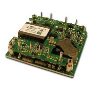
JNC350R41-TZ
Manufacturer Part Number
JNC350R41-TZ
Description
DC/DC Converters & Regulators 350W 24V-28V 12.5A NegLogic TunableLoop
Manufacturer
Lineage Power
Datasheet
1.JNC350R41-TZ.pdf
(16 pages)
Specifications of JNC350R41-TZ
Output Power
350 W
Input Voltage Range
18 V to 36 V
Input Voltage (nominal)
24 V
Output Voltage (channel 1)
28 V
Output Current (channel 1)
12.5 A
Package / Case Size
Half Brick
Output Voltage
28 V
Product
Isolated
Lead Free Status / RoHS Status
Lead free / RoHS Compliant
Other names
CC109158457


August 9, 2010
Electrical Specifications
1. For Vin ≤ 19V, and case temperatures ≥ 85°C, output voltage regulation is relaxed to -2
2. When operating at output current between 0A
3. Use a minimum 2 x 220uF output capacitor. Recommended capacitor is Nichicon CD series, 220uF/35V. If the ambient
temperature is less than 0°C, use 3x of the minimum C
4. External capacitors may require using the new Tunable Loop™ feature to ensure that the module is stable as well as getting the
best transient response. See the Tunable Loop™ section for details.
Isolation Specifications
General Specifications
LINEAGE
Parameter
Isolation Capacitance
Isolation Resistance
Parameter
Output Voltage Set-point
(V
Output Voltage
(Over all operating input voltage, resistive load,
and temperature conditions until end of life)
Output Regulation
Output Ripple and Noise on nominal output
External Capacitance
Without the Tunable Loop™
With the Tunable Loop™
Output Current
Output Current Limit Inception
Output Short Circuit Current (V
Efficiency
V
Switching Frequency
Dynamic Load Response
Parameter
Calculated Reliability based upon Telcordia SR-
332 Issue 2: Method
T
Weight
A
Line (V
Load (I
Temperature (T
(V
IN
IN
=40°C, airflow = 200 lfm, 90% confidence)
=V
RMS (5Hz to 20MHz bandwidth)
Peak-to-Peak (5Hz to 20MHz bandwidth)
Load Change from Io= 50% to 75% of Io,max:
Load Change from Io= 25% to 50% of Io,max:
=V
(Io/t=1A/10s; V
with a 470 μF aluminum and a 10 µF ceramic
IN
=V
IN, nom
IN,nom
IN, nom
IN
O
POWER
=I
Settling Time (Vo<10% peak deviation)
Settling Time (Vo<10% peak deviation)
=V
, T
, I
O, min
O
IN, min
c
and I
=I
=25°C I
1
2
O, max
to I
c
to V
= -40ºC to +100ºC)
O
O, max
=I
, T
I
O
O, min
IN, max
(ESR > 50 mΩ)
capacitor across the load.)
Case 3 (I
=I
in
c
=V
)
=25°C)
O, max ,
1
(ESR > 50 mΩ)
to I
in
)
,
nom
(ESR
O, max
V
O
; T
O
≤ 0.25V
O
=80%I
= V
MAX
c
Peak Deviation
Peak Deviation
)
=25°C; Tested
3
O,set
= 80mΩ)
(continued)
4
O, max
dc
)
,
2
3
dc
and 1A
All, except
Device
Device
O
All
All
.
All
All
All
All
All
All
All
All
All
All
All
All
-T
-T
-T
18 – 36 Vdc Input; 28Vdc Output; 350W Output
dc
, output ripple may exceed maximum pk-pk limits.
Symbol
Symbol
MTBF
Symbol
C
R
FIT
V
I
I
iso
iso
O, lim
V
V
C
C
C
O, sc
V
f
O, set
I
t
t
η
sw
o
pk
s
pk
s
O
O
O
O
Min
Min
10
27.15
27.5
13.1
Min
440
440
440
0
.
5%V
2,925,365
341.8
o,set
Typ
Typ
2.8
15
78
Typ
300
0.1
0.1
0.5
1.5
1.5
28
45
80
91
.
2
2
28.85
8,000
6500
Max
Max
28.5
12.5
17.5
Max
200
470
0.2
0.2
1.5
55
30
10
%V
%V
%V
%V
%V
mV
mV
Hours
Unit
9
A
kHz
Unit
V
A
A
ms
ms
μF
μF
μF
Unit
/Hours
oz.
%
MΩ
V
nF
rms
g
O, set
O, set
dc
pk-pk
dc
dc
o,set
o,set
o,set
rms
dc
3
Related parts for JNC350R41-TZ
Image
Part Number
Description
Manufacturer
Datasheet
Request
R

Part Number:
Description:
Manufacturer:
Lineage Power
Datasheet: