CP2112EK Silicon Laboratories Inc, CP2112EK Datasheet
CP2112EK
Specifications of CP2112EK
Available stocks


Related parts for CP2112EK


CP2112EK Summary of contents
Page 1
HID USB INGLE H IP Single-Chip HID USB to SMBus Master Bridge Integrated USB transceiver; no external resistors required SMBus master device GPIO can be configured as Input/Output and Open- Drain/Push-Pull 512 Byte SMBus ...
Page 2
CP2112 2 Rev. 1.0 ...
Page 3
T C ABLE O F ONTENTS Section 1. System Overview . . . . . . . . . . . . . . . . . . . . . . . . . . . . . . ...
Page 4
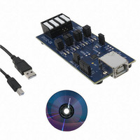
... MHz to 94 kHz) and TX and RX LED toggle. Support for I/O interface voltages down to 1 provided via evaluation kit for the CP2112 (Part Number: CP2112EK) is available. It includes a CP2112-based HID USB-to- SMBus evaluation board, Windows DLL and test application, USB cable, and full documentation www ...
Page 5
Electrical Characteristics Table 1. Absolute Maximum Ratings Parameter Ambient Temperature under Bias Storage Temperature Voltage on RST, SDA, SCL, or GPIO Pins with respect to GND Voltage with respect to GND DD IO Maximum Total ...
Page 6
CP2112 Table 3. SMBus, Suspend I/O DC Electrical Characteristics V = 3 –40 to +85 °C unless otherwise specified Parameters Output High Voltage ( Output ...
Page 7
Pinout and Package Definitions Name Pin # Type V 6 Power In DD Power Out V 5 Power In I/O Supply Voltage Input. IO GND 2 RST 9 D I/O REGIN 7 Power Regulator Input. This ...
Page 8
CP2112 Table 7. CP2112 Pin Definitions (Continued) Name Pin # Type SUSPEND 11* D Out SUSPEND 17* D Out NC 18*, 19* NC 10* *Note: Pins can be left unconnected when not in use. 8 Description This pin is logic ...
Page 9
SDA 1 GND CP2112-GM Top View D- 4 VIO 5 GND (optional) VDD 6 Figure 2. QFN-24 Pinout Diagram (Top View) Rev. 1.0 CP2112 SUSPEND 16 VPP 15 GPIO.4 14 GPIO.5 13 GPIO.6 9 ...
Page 10
CP2112 4. QFN-24 Package Specifications Table 8. QFN-24 Package Dimensions Dimension Min A 0.70 A1 0.00 b 0.18 D 4.00 BSC. D2 2.55 e 0.50 BSC. E 4.00 BSC. E2 2.55 Notes: 1. All dimensions shown are in millimeters (mm) ...
Page 11
Figure 4. QFN-24 Recommended PCB Land Pattern Table 9. QFN-24 PCB Land Pattern Dimensions Dimension Min Max C1 3.90 4.00 C2 3.90 4.00 E 0.50 BSC X1 0.20 0.30 Notes: General 1. All dimensions shown are in millimeters (mm) unless ...
Page 12
CP2112 5. USB Function Controller and Transceiver The Universal Serial Bus (USB) function controller in the CP2112 is a USB 2.0 compliant full-speed device with integrated transceiver and on-chip matching and pullup resistors. The USB function controller manages all data ...
Page 13
SMBus Operation Two types of data transfers are possible: data transfers from a master transmitter to an addressed slave receiver (WRITE) and data transfers from an addressed slave transmitter to a master receiver (READ). The master device initiates both ...
Page 14
CP2112 7. GPIO Pins The CP2112 supports 8 user-configurable GPIO pins. Each of these GPIO pins are usable as inputs, open-drain outputs, or push-pull outputs. Three of these GPIO pins also have alternate functions which are listed in Table 10. ...
Page 15
One-Time Programmable ROM The CP2112 includes an internal, one-time programmable ROM that may be used to customize the USB vendor ID (VID), product ID (PID), manufacturer string, product description string, power descriptor, device release number, and device serial number ...
Page 16
CP2112 9. Voltage Regulator The CP2112 includes an on-chip 5.0 to 3.45 V voltage regulator. This allows the CP2112 to be configured as either a USB bus-powered device or a USB self-powered device. A typical connection diagram of the device ...
Page 17
Alternatively, if 3.0 to 3.6 V power is supplied to the V device with the voltage regulator bypassed. For this configuration, tie the REGIN input to V regulator. A typical connection diagram showing the device in a self-powered application with ...
Page 18
... A Windows DLL that encapsulates the CP2112 HID interface and also adds higher level features, such as read/ write timeouts is provided by Silicon Labs. This DLL is the recommended interface for the CP2112. The Windows DLL is documented in CP2112 Windows DLL Specification. Both of these documents and the DLL are available in the CP2112EK CD as well as online at http://www.silabs.com/. 11. Relevant Application Notes The following Application Notes are applicable to the CP2112 ...
Page 19
OCUMENT HANGE IST Revision 0.1 to Revision 0.5 Updated Table 3 on page 6. Updated Table 4 on page 6. Updated Table 5 on page 6. Updated Table 11 on page 15. Revision ...
Page 20
... Should Buyer purchase or use Silicon Laboratories products for any such unintended or unauthorized application, Buyer shall indemnify and hold Silicon Laboratories harmless against all claims and damages. Silicon Laboratories, Silicon Labs, and USBXpress are trademarks of Silicon Laboratories Inc. Other products or brandnames mentioned herein are trademarks or registered trademarks of their respective holders 20 Rev ...