XC2C384-10TQG144C Xilinx Inc, XC2C384-10TQG144C Datasheet
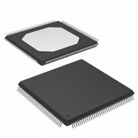
IC, CPLD, 384 MACROCELL, 7.1NS, TQFP-144

XC2C384-10TQG144C

Manufacturer Part Number
XC2C384-10TQG144C
Description
IC, CPLD, 384 MACROCELL, 7.1NS, TQFP-144
Manufacturer
Xilinx Inc
Series
CoolRunner IIr
Datasheets

Specifications of XC2C384-10TQG144C

No. Of Macrocells
384
No. Of I/o's
118
Propagation Delay
7.1ns
Global Clock Setup Time
3.3ns
Frequency
125MHz
Supply Voltage Range
1.7V To 1.9V
Programmable Type
In System Programmable
Delay Time Tpd(1) Max
9.2ns
Voltage Supply - Internal
1.7 V ~ 1.9 V
Number Of Logic Elements/blocks
24
Number Of Macrocells
384
Number Of Gates
9000
Number Of I /o
118
Operating Temperature
0°C ~ 70°C
Mounting Type
Surface Mount
Package / Case
144-TQFP, 144-VQFP
Features
JTAG
Voltage
1.8V
Memory Type
CMOS
Rohs Compliant
Yes
Lead Free Status / RoHS Status
Lead free / RoHS Compliant
Number Of Logic Elements/cells
-
Lead Free Status / RoHS Status
Lead free / RoHS Compliant, Lead free / RoHS Compliant
Other names
122-1406

Available stocks

Company
Part Number
Manufacturer
Quantity
Price
Part Number:
XC2C384-10TQG144C
Manufacturer:
XILINX
Quantity:
214
Part Number:
XC2C384-10TQG144C
Manufacturer:
XILINX
Quantity:
455
Part Number:
XC2C384-10TQG144C
Manufacturer:
Xilinx Inc
Quantity:
10 000
Part Number:
XC2C384-10TQG144C
Manufacturer:
XILINX
0
DS090 (v3.1) September 11, 2008
Features
Table 1: CoolRunner-II CPLD Family Parameters
DS090 (v3.1) September 11, 2008
Product Specification
Macrocells
Max I/O
T
T
T
F
PD
SU
CO
SYSTEM1
© 2002–2008 Xilinx, Inc. All rights reserved. All Xilinx trademarks, registered trademarks, patents, and disclaimers are as listed at http://www.xilinx.com/legal.htm.
Optimized for 1.8V systems
-
-
Industry’s best 0.18 micron CMOS CPLD
-
-
Advanced system features
-
-
-
-
-
-
-
-
-
-
-
-
-
-
-
(ns)
(ns)
(ns)
Industry’s fastest low power CPLD
Densities from 32 to 512 macrocells
Optimized architecture for effective logic synthesis
Multi-voltage I/O operation — 1.5V to 3.3V
Fastest in system programming
·
On-The-Fly Reconfiguration (OTF)
IEEE1149.1 JTAG Boundary Scan Test
Optional Schmitt trigger input (per pin)
Multiple I/O banks on all devices
Unsurpassed low power management
·
Flexible clocking modes
·
·
·
Global signal options with macrocell control
·
·
·
Abundant product term clocks, output enables and
set/resets
Efficient control term clocks, output enables and
set/resets for each macrocell and shared across
function blocks
Advanced design security
Open-drain output option for Wired-OR and LED
drive
Optional bus-hold, 3-state or weak pullup on select
I/O pins
Optional configurable grounds on unused I/Os
Mixed I/O voltages compatible with 1.5V, 1.8V,
2.5V, and 3.3V logic levels on all parts
All other trademarks and registered trademarks are the property of their respective owners. All specifications are subject to change without notice.
(MHz)
1.8V ISP using IEEE 1532 (JTAG) interface
DataGATE external signal control
Optional DualEDGE triggered registers
Clock divider (÷ 2,4,6,8,10,12,14,16)
CoolCLOCK
Multiple global clocks with phase selection per
macrocell
Multiple global output enables
Global set/reset
XC2C32A
323
3.8
1.9
3.7
32
33
R
XC2C64A
263
4.6
2.0
3.9
64
64
0
0
www.xilinx.com
XC2C128
0
128
100
244
5.7
2.4
4.2
CoolRunner-II CPLD Family
Product Specification
Family Overview
Xilinx CoolRunner™-II CPLDs deliver the high speed and
ease of use associated with the XC9500/XL/XV CPLD fam-
ily with the extremely low power versatility of the XPLA3
family in a single CPLD. This means that the exact same
parts can be used for high-speed data communications/
computing systems and leading edge portable products,
with the added benefit of In System Programming. Low
power consumption and high-speed operation are com-
bined into a single family that is easy to use and cost effec-
tive. Clocking techniques and other power saving features
extend the users’ power budget. The design features are
supported starting with Xilinx ISE® 4.1i WebPACK tool.
Additional details can be found in
page
Table 1
parameters for the CoolRunner-II CPLD family.
-
-
PLA architecture
-
-
Wide package availability including fine pitch:
-
-
Design entry/verification using Xilinx and industry
standard CAE tools
Free software support for all densities using Xilinx®
WebPACK™ tool
Industry leading nonvolatile 0.18 micron CMOS
process
-
-
14.
SSTL2_1,SSTL3_1, and HSTL_1 on 128
macrocell and denser devices
Hot pluggable
Superior pinout retention
100% product term routability across function block
Chip Scale Package (CSP) BGA, Fine Line BGA,
TQFP, PQFP, VQFP, and QFN packages
Pb-free available for all packages
Guaranteed 1,000 program/erase cycles
Guaranteed 20 year data retention
shows the macrocell capacity and key timing
XC2C256
256
184
256
5.7
2.4
4.5
XC2C384
384
240
217
7.1
2.9
5.8
Further Reading,
XC2C512
512
270
179
7.1
2.6
5.8
1

Related parts for XC2C384-10TQG144C

XC2C384-10TQG144C Summary of contents

Page 1

... CoolRunner-II CPLD family. XC2C64A XC2C128 XC2C256 64 128 64 100 4.6 5.7 2.0 2.4 3.9 4.2 263 244 www.xilinx.com Further Reading, XC2C384 XC2C512 256 384 512 184 240 270 5.7 7.1 7.1 2.4 2.9 2.6 4.5 5.8 5.8 256 217 ...

Page 2

... I/O banks are needed on 32 and 64 macrocell parts, but very likely they are for 384 and 512 macrocell parts. The I/O banks are groupings of I/O pins using any one of a subset of compatible voltage standards that share www.xilinx.com XC2C256 XC2C384 XC2C512 ...

Page 3

... Figure 1 attach to pins and interconnect to each other within the internal interconnect matrix. Each FB contains 16 macro- cells. The BSC path is the JTAG Boundary Scan Control www.xilinx.com CoolRunner-II CPLD Family XC2C384 XC2C512 ✓ ✓ ✓ ✓ ...

Page 4

CoolRunner-II CPLD Family path. The BSC and ISP block has the JTAG controller and In-System Programming Circuits. MC1 I/O Pin MC2 I/O Pin 16 MC16 I/O Pin 16 JTAG BSC and ISP Function Block The CoolRunner-II CPLD FBs contain 16 ...

Page 5

R Macrocell The CoolRunner-II CPLD macrocell is extremely efficient and streamlined for logic creation. Users can develop sum of product (SOP) logic expressions that comprise inputs and span 56 product terms within a single function block. The ...

Page 6

CoolRunner-II CPLD Family software. The AIM minimizes both propagation delay and power as it makes attachments to the various FBs. I/O Block I/O blocks are primarily transceivers. However, each I/O is either automatically compliant with standard voltage ranges or can ...

Page 7

R Output Banking CPLDs are widely used as voltage interface translators. To that end, the output pins are grouped in large banks. The XC2C32A, XC2C64A, XC2C128 and XC2C256 devices support two output banks. With two, the outputs switch to one ...

Page 8

CoolRunner-II CPLD Family nally generated DataGATE control logic can be assigned to this I/O pin with the BUFG=DATA_GATE attribute. Latch Latch Figure 6: DataGATE Architecture (output drivers not shown) Global Signals Global signals, clocks (GCK), sets/resets (GSR), and output enables ...

Page 9

R Additional Clock Options: Division, DualEDGE, and CoolCLOCK Clock Divider A clock divider circuit has been included in the CoolRunner-II CPLD architecture to divide one externally supplied global clock by standard values. The allowable val- ues for the division are ...

Page 10

CoolRunner-II CPLD Family CLK_CT PTC Figure 9: Macrocell Clock Chain with DualEDGE Option Shown GCK2 Synch Reset Figure 10: CoolCLOCK Created by Cascading Clock Divider and DualEDGE Option Design Security Designs can be secured during programming to prevent either accidental ...

Page 11

R Timing Model Figure 11 shows the CoolRunner-II CPLD timing model. It represents one aspect of the overall architecture from a tim- ing viewpoint. Each little block is a time delay that a signal incurs if the signal passes through ...

Page 12

CoolRunner-II CPLD Family Programming The programming data sequence is delivered to the device using either Xilinx iMPACT software and a Xilinx download cable, a third-party JTAG development JTAG-compatible board tester simple microprocessor interface that emulates the JTAG instruction ...

Page 13

programmed at any time. All devices are shipped in the erased state from the factory. Applying power to a blank part might result in a higher cur- rent flow as the part initializes. This behavior is normal ...

Page 14

CoolRunner-II CPLD Family Absolute Maximum Ratings Symbol (2) V Supply voltage relative to GND CC (3) V Input voltage relative to GND I T Ambient Temperature (C-grade) A Ambient Temperature (I-grade) (4) T Maximum junction temperature J T Storage temperature ...

Page 15

... Data Sheet) s311.pdf http://www.xilinx.com/support/documentation/data_sheets/d (XC2C128 Data Sheet) s093.pdf http://www.xilinx.com/support/documentation/data_sheets/d (XC2C256 Data Sheet) s094.pdf http://www.xilinx.com/support/documentation/data_sh eets/ds095.pdf (XC2C384 Data Sheet) http://www.xilinx.com/support/documentation/data_sheets/d (XC2C512 Data Sheet) s096.pdf CoolRunner-II CPLD White Papers http://www.xilinx.com/support/documenta- tion/white_papers/wp170.pdf Packages Package Drawings Revision specification. ...

Page 16

CoolRunner-II CPLD Family Date Version 04/15/05 2.4 Change to F 06/28/05 2.5 Move to Product Specification 03/20/06 2.6 Add Warranty Disclaimer; modified Global Signals section to say that GCK, GSR and GTS can be used as general purpose I/O. 07/24/06 ...

Related keywords