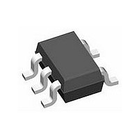
LMV7271MG National Semiconductor, LMV7271MG Datasheet - Page 10

LMV7271MG
Manufacturer Part Number
LMV7271MG
Description
IC,VOLT COMPARATOR,SINGLE,TSSOP,5PIN,PLASTIC
Manufacturer
National Semiconductor
Datasheet
1.LMV7271MG.pdf
(18 pages)
Specifications of LMV7271MG
Rohs Compliant
NO
Number Of Elements
1
Output Type
Push-Pull
Technology
BiCMOS
Input Offset Voltage
4mV
Input Bias Current (typ)
10nA
Single Supply Voltage (typ)
3/5V
Dual Supply Voltage (typ)
Not RequiredV
Supply Current (max)
0.014mA
Power Supply Requirement
Single
Common Mode Rejection Ratio
78dB
Power Supply Rejection Ratio
80dB
Single Supply Voltage (min)
1.8V
Single Supply Voltage (max)
5.5V
Dual Supply Voltage (min)
Not RequiredV
Dual Supply Voltage (max)
Not RequiredV
Operating Temp Range
-40C to 85C
Operating Temperature Classification
Industrial
Mounting
Surface Mount
Pin Count
5
Package Type
SC-70
Lead Free Status / Rohs Status
Not Compliant
Available stocks
Company
Part Number
Manufacturer
Quantity
Price
Part Number:
LMV7271MG
Manufacturer:
NS/国半
Quantity:
20 000
Company:
Part Number:
LMV7271MGX
Manufacturer:
NS
Quantity:
9 000
Company:
Part Number:
LMV7271MGX
Manufacturer:
FAIRCHILD
Quantity:
840
Part Number:
LMV7271MGX
Manufacturer:
NS/国半
Quantity:
20 000
Part Number:
LMV7271MGX/NOPB
Manufacturer:
TI/德州仪器
Quantity:
20 000
www.national.com
Application Notes
BASIC COMPARATOR
A comparator is often used to convert an analog signal to a
digital signal. As shown in
an input voltage (V
RAIL-TO-RAIL INPUT STAGE
The LMV727X has an input common mode voltage range
(V
achieved by using paralleled PNP and NPN differential input
pairs. When the V
PNP pair is off. When the V
and the PNP pair is on. The crossover point between the NPN
and PNP input stages is around 950mV from V
input stage has its own offset voltage (V
comparator becomes a function of the V
V
In application design, it is recommended to keep the V
away from the crossover point to avoid problems. The wide
input voltage range makes LMV727X ideal in power supply
monitoring circuits, where the comparators are used to sense
signals close to ground and power supplies.
OUTPUT STAGE
The LMV7271 and LMV7272 have a push-pull output stage.
This output stage keeps the total system power consumption
to the absolute minimum. The only current consumed is the
low supply current and the current going directly into the load.
When the output switches, both PMOS and NMOS at the out-
put stage are on at the same time for a very short time. This
allows current to flow directly between V
put transistors. The result is a short spike of current (shoot-
through current) drawn from the supply and glitches in the
supply voltages. The glitches can spread to other parts of the
board as noise. To prevent the glitches in supply lines, power
supply bypass capacitors must be installed. See section for
supply bypassing in the Application Notes for details.
HYSTERESIS
It is a standard procedure to use hysteresis (positive feed-
back) around a comparator, to prevent oscillation, and to
OS
CM
vs. V
) of −0.1V below the V
CM
in Typical Performance Characteristics section.
CM
IN
) to a reference voltage (V
is near V
Figure
LMV7271
CM
−
+
is near V
, the NPN pair is on and the
to 0.1V above V
2, the comparator compares
+
−
, the NPN pair is off
and V
OS
CM
20064025
FIGURE 2. LMV7271 Basic Comparator
), the V
. See curves for
−
+
REF
. Since each
through out-
+
). If V
. This is
OS
of the
IN
CM
is
10
less than V
greater than V
avoid excessive noise on the output because the comparator
is a good amplifier of its own noise.
Inverting Comparator with Hysteresis
The inverting comparator with hysteresis requires a three re-
sistor network that is referenced to the supply voltage V
the comparator
less than V
comparator (V
assume V
sistors can be represented as R
lower input trip voltage V
When V
low and very close to ground. In this case the three network
resistors can be presented as R
upper trip voltage V
The total hysteresis provided by the network is defined as
A good typical value of ΔV
50mV. This is easily obtained by choosing R
times (R
R
2
) for 1.8V operation.
IN
1
||R
O
is greater than V
A
REF
switches as high as V
2
, the voltage at the non-inverting node of the
) for 5V operation, or as 300 to 30 times (R
IN
REF
, the output (V
(Figure
< V
, the output voltage (V
A
A2
), the output voltage is high (for simplicity
is defined as
ΔV
3). When V
A1
A
A
= V
is defined as
A
(V
would be in the range of 5 to
A1
O
IN
) is low. However, if V
1
2
- V
> V
//R
||R
CC
IN
A2
). The three network re-
3
3
A
at the inverting input is
), the output voltage is
in series with R
in series with R
O
) is high.
3
as 1000 to 100
20064017
2
1
. The
. The
CC
IN
1
of
is
||


