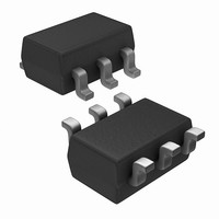
TLE4917 Infineon Technologies, TLE4917 Datasheet

TLE4917
Specifications of TLE4917
TLE4917XT
TLE4917XT
Available stocks
Related parts for TLE4917
TLE4917 Summary of contents
Page 1
Low Power Hall Switch Features Micro power design 2 5.5 V battery operation High sensitivity and high stability of the magnetic switching points High resistance to mechanical stress Digital output signal Switching for both poles of a magnet ...
Page 2
Pin Configuration (top view) Sensitive Area Figure 1 Pin Definitions and Functions Pin Symbol GND GND 5 GND 6 PRG Data Sheet Top View PRG GND GND ...
Page 3
Active Error Compensation Hall Probe Chopped Amplifier Figure 2 Block Diagram Circuit Description The Low Power Hall IC Switch comprises a Hall probe, bias generator, compensation circuits, oscillator, output latch and an n-channel open drain output transistor. The bias generator ...
Page 4
In that case the output Q is off at high magnetic fields and no current is flowing in the open drain transistor. The output transistor can sink with a maximal saturation voltage V Absolute ...
Page 5
Operating Range Parameter Symbol Supply voltage V Output voltage V Programming Pin Voltage V Ambient Temperature Ceramic Bypass Capacitor AC/DC Characteristics Parameter Symbol Averaged Supply Current I Averaged Supply I Current during Operating ...
Page 6
Magnetic Characteristics PRG Pin Connected Parameter Symbol Operate Points B B Release Points B B Hysteresis B 1) Positive magnetic fields are related to the approach of a magnetic south pole to the branded side of package ...
Page 7
SOPAVG I SAVG I SSTB Figure 3 Timing Diagram Figure 4 Programming of Output with the PRG Pin Data Sheet Operating Time Standby Time stb 130 Latch t Output AET02802-17 ...
Page 8
All curves reflect typical values at the given parameters for T Magnetic Switching Points versus Temperature (V =2.7V) S (PRG Pin Connected to V B[mT -40 - Supply current ...
Page 9
Supply current I during Standby SSTB Time versus Temperature ( [µ -40 - Output Saturation voltage V versus Temperature ( I =1mA ) Q 200 ...
Page 10
Top View Direction of Unreeling Package P-TSOP6-6-2 Figure 5 Marking and Tape Loading Orientation Figure 6 Foot Print Reflow Soldering Data Sheet Marking on P-TSOP6-6-2 package corresponds to pin 1 of device ...
Page 11
Package Dimensions P-TSOP6-6-2 (Plastic Thin Small Outline-Package) weight : 0.015g coplanary : 0.1mm Sorts of Packing Package outlines for tubes, trays etc. are contained in our Data Book ”Package Information”. SMD = Surface Mounted Device Data Sheet 11 Dimensions in ...
Page 12
Information about the application circuit of the TLE 4917 1 Vs TLE 4917 2 Gnd 3 Q Application circuit TLE 4917 The minimum value for the pull up resistor can be calculated with the power supply voltage Vs, the maximum ...
Page 13
... Due to technical requirements components may contain dangerous substances. For information on the types in question please contact your nearest Infineon Technologies Office. Infineon Technologies Components may only be used in life-support devices or systems with the express written approval of Infineon Technologies failure of such components can reasonably be expected to cause the failure of that life-support device or system affect the safety or effectiveness of that device or system ...


