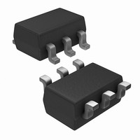
TLE4966H Infineon Technologies, TLE4966H Datasheet

TLE4966H
Specifications of TLE4966H
TLE4966HXT
TLE4966HXT
Related parts for TLE4966H
TLE4966H Summary of contents
Page 1
TLE4966L High Precision Hall-Effect Switch with Direction Detection Data Sheet, V 2.0, February 2009 ...
Page 2
... Infineon Technologies Office. Infineon Technologies components may be used in life-support devices or systems only with the express written approval of Infineon Technologies failure of such components can reasonably be expected to cause the failure of that life-support device or system or to affect the safety or effectiveness of that device or system. Life support devices or systems are intended to be implanted in the human body or to support and/or maintain and sustain and/or protect human life ...
Page 3
... Revision History: Previous Version: Page Subjects (major changes since last revision) TLE4966H removed We Listen to Your Comments Any information within this document that you feel is wrong, unclear or missing at all? Your feedback will help us to continuously improve the quality of this document. Please send your proposal (including a reference to this document) to: sensors@infineon ...
Page 4
Overview . . . . . . . . . . . . . . . . . . . . . . . . . . . . . . . . . . . . . . ...
Page 5
High Precision Hall-Effect Switch with Direction Detection 1 Overview 1.1 Features • 2 supply voltage operation • Operation from unregulated power supply • High sensitivity and high stability of the magnetic switching points • High resistance ...
Page 6
Pin Configuration (top view) Center of Sensitive Area Figure 1 Pin Definition and Center of Sensitive Area Table 1 Pin Definitions and Functions Pin No. Symbol GND Data Sheet 1.45 2.67 ...
Page 7
General 2.1 Block Diagram Voltage Regulator (reverse polarity protected ) Oscillator & Sequencer Amplifier Chopped Hall Probe Amplifier Chopped Hall Probe Figure 2 Block Diagram 2.2 Circuit Description The chopped Double Hall Switch comprises two Hall probes, bias generator, ...
Page 8
Maximum Ratings Table 2 Absolute Maximum Ratings T = -40°C to 150°C j Parameter Symbol V Supply voltage S I Supply current S through protection device V Output voltage Q I Continuous Q output current T Junction j temperature ...
Page 9
Operating Range Table 4 Operating Range Parameter Symbol V Supply voltage S V Output voltage Q T Junction j temperature I Output current Q Data Sheet Limit Values min. typ. max. 2.7 – 18 – – 24 – – ...
Page 10
Electrical and Magnetic Parameters Table 5 Electrical Characteristics Parameter Symbol I Supply current S I Reverse current SR V Output saturation voltage I Output leakage QLEAK current t Output fall time f t Output rise time r f Chopper ...
Page 11
Calculation of the ambient temperature e.g. for = 12 Styp P Power Dissipation: = 72.0 mW. DIS – 175°C – (190 K thJA DIS Resulting ...
Page 12
Timing Diagrams for the Speed and Direction Outputs Applied Magnetic Field 90% 10% Figure 3 Timing Definition of the Speed Signal Speed Direction Figure 4 Timing Definition of the Direction Signal Data Sheet ...
Page 13
N S Figure 5 Definition of the Direction Signal Rotation Direction Left to right Right to left Data Sheet Timing Diagrams for the Speed and Direction Outputs Rotation Direction TLE4966 State of ...
Page 14
Package Information 7.1 Package Marking Figure 6 Marking PG-SSO-4-1 Figure 7 Marking 7.2 Distance between Chip and Package Surface Figure 8 Distance Chip to Upper Side of IC Data Sheet Year (yy ... 99 Calendar Week (ww) ...
Page 15
Package Outlines Figure 9 PG-SSO-4-1 5.34 ±0.05 5.16 ±0.08 1.9 MAX. CODE 1 4 1.27 6.35 ±0.4 Total tolerance at 10 pitches ± solder function area You can find all of our packages, sorts of packing and ...
Page 16
... Published by Infineon Technologies AG ...


